Hi TI Experts,
I have the below queries on using the Ethernet interface peripherals in my design.
1.Peripherals Supporting Ethernet interface
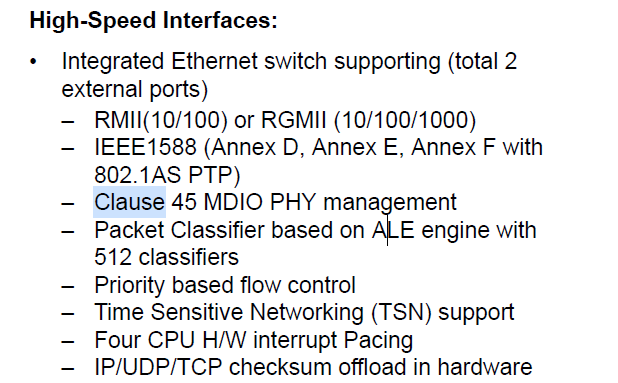
2.Number of Ethernet interfaces supported by CPSW3G
3.Number of Instances and Ethernet interfaces supported by PRU_ICSSG
4.Are all 6 Ethernet interfaces supported by any of the AM64x family of devices
5.Does all the devices in the Family support the same number of Ethernet interfaces?
6.What PRU_ICSSG functionality is on each AM64x device
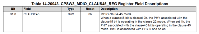
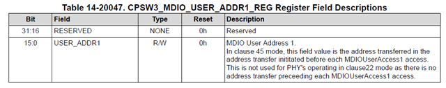
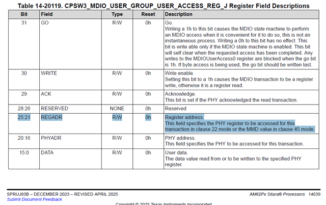
7.Any recommendation for using MDIO interfaces
8.Is AM64x affected by the MDIO Errata
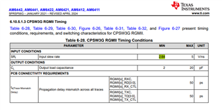
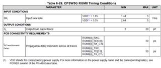
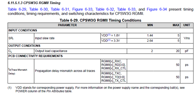
9.Do you have recommendations on adding series resistors for RGMII interface
10.Are the above series resistor recommendations valid for MII or RMII interface
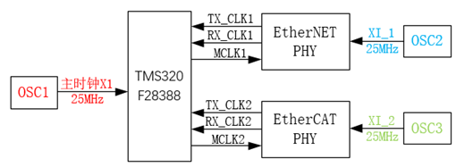
11.Is there any clock recommendations When using Ethernet interface
12.Recommendations for using External clock oscillator
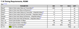
13.IO levels supported for Ethernet interface
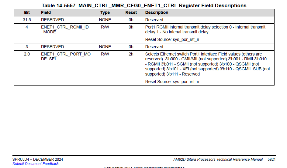
14.Is the RGMII internal delay supported by the processor and is the RGMII internal delay configurable
15.Can AM64x CPSW handle both 100BASE RMII for one port and 1000BASE RGMII for another port?
16. Can i interface 2 X RMII PHYs with the PHY configured as Master
17. Do you have interfacing recommendations for RMII interface
Let me know your thoughts.