This thread has been locked.

If you have a related question, please click the "Ask a related question" button in the top right corner. The newly created question will be automatically linked to this question.

[FAQ] AM625 / AM623 / AM620-Q1 / AM62L / AM62Ax / AM62D-Q1 / AM62Px / AM64x / AM243x (ALV) Design Recommendations / Commonly Observed Errors during Custom board hardware design – DDRSS : DDR4 / LPDDR4 MEMORY Interface

Other Parts Discussed in Thread: AM62L, AM62D-Q1, SK-AM62, SK-AM62B-P1, AM625, AM62P, TPS51200, SK-AM64B, PROCESSOR-SDK-AM62X, SITARA-DDR-CONFIG-TOOL, AM625-Q1, AM623, AM620-Q1, SYSCONFIG, AM6442, TDA4VM, AM62A7, AM62A7-Q1, SK-AM62P-LP, TDA4VH, AM67, SK-AM68, TMDS62LEVM, TMDS64EVM, SK-AM62-LP, AM6412, AM62P-Q1, TDA4VE-Q1

Hi TI Experts,

Is there a list of design recommendations or commonly observed errors for DDR4 / LPDDR4 MEMORY Interface during Custom board hardware design?

Thank you.

https://www.google.com/search?q=james+TI+ddr+config+video&sca_esv=21f0f7159a2b44ff&rlz=1C1CHBF_enIN1030IN1030&sxsrf=ANbL-n6tJufu8SySWP0BkHMUgdsoqEDinA%3A1776252369081&ei=0XXfac3WBL6gseMPmKLFoQg&biw=1163&bih=532&ved=0ahUKEwiNg_bb3--TAxU-UGwGHRhRMYQQ4dUDCBE&uact=5&oq=james+TI+ddr+config+video&gs_lp=Egxnd3Mtd2l6LXNlcnAiGWphbWVzIFRJIGRkciBjb25maWcgdmlkZW8yCBAhGKABGMMEMggQIRigARjDBEj9KFDyCVjwIXABeACQAQCYAaYFoAHsHaoBCzAuMi40LjEuMi4yuAEDyAEA-AEBmAIGoAKeDMICCBAAGO8FGLADwgILEAAYgAQYogQYsAPCAgUQABjvBcICCBAAGIAEGKIEmAMAiAYBkAYEkgcJMS4xLjMuNS0xoAf4HbIHCTAuMS4zLjUtMbgHgwzCBwcyLTQuMS4xyAcygAgB&sclient=gws-wiz-serp#fpstate=ive&vld=cid:378a314c,vid:FF8OiiktRjU,st:0

/cfs-file/__key/communityserver-discussions-components-files/791/JESD79_2D00_4.pdf

/cfs-file/__key/communityserver-discussions-components-files/791/2806.schematic.pdf

Memory Device Search Key words

NOR and NAND Flash Cross Reference Guide

NOR NAND Flash Guide

 (+) AM62A7: List of recommended Flash and Ram - Processors forum - Processors - TI E2E support forums

DDR configuration

https://dev.ti.com/tirex/content/Processor_DDR_Config_0.10.40.0000/docs/README.html

 https://dev.ti.com/sysconfig/?product=Processor_DDR_Config&device=AM62x

https://dev.ti.com/sysconfig/?product=Processor_DDR_Config&device=AM62Ax

  • Hi Board designers, 

    Here are some of the commonly observed errors and recommendations for DDR4 / LPDDR4 MEMORY Interface during Custom board hardware design.

    Recommendations 

    1. DDR design guide 

    AM64x

    DDR Board Design and Layout Guidelines
    https://www.ti.com/lit/pdf/spracu1


    DDR Board Design and Layout Guidelines for AM62x/AM62L can be additionally referenced
    www.ti.com/.../sprad06

    AM62x / AM62L

    https://www.ti.com/lit/an/sprad06/sprad06.pdf

    AM62Ax and AM62Px

    https://www.ti.com/lit/an/sprad66a/sprad66a.pdf

    1. Supported Memory Type, Memory Size, Speed and Type,

    Refer to the processor specific data sheet.

    AM64x / AM243x (ALV)

    https://www.ti.com/product/AM2432

    https://www.ti.com/product/AM6442

    DDR4, LPDDR4

    AM62x

    https://www.ti.com/lit/gpn/am625

    DDR4, LPDDR4

    AM62L 

    www.ti.com/.../AM62L

    DDR4, LPDDR4

    Note on DDR4 support for Am62L:

    Refer to AM64x or the AM62x SK or EVM for DDR4 interface implementation.

    DDR Configuration for AM62Lx, they can use the AM62x tool.  This has the same DDR controller and PHY as AM62L

    1) Currently no SDK/driver support available as there is no EVM to validate this
    2) We are evaluating how to have some bare minimum support for DDR4, but this will likely be a couple of months of effort *however* even if we do this there will be no support for low power modes with DDR4 until we have a robust EVM like platform for SDK teams to offer full support

    Check the documentation on TI.com for the available support. 

    AM62Ax
    https://www.ti.com/lit/gpn/am62a7

    LPDDR4

    AM62D-Q1

    https://www.ti.com/lit/gpn/am62D-Q1 

    LPDDR4

    AM62Px

    https://www.ti.com/lit/gpn/am62p

    LPDDR4

    Reference Links 

    https://e2e.ti.com/support/processors-group/processors/f/processors-forum/1278830/am625-am625-8bit-single-rank-ddr4-chip-x-2pcs-support

    (+) AM625: DDR CLK termination specification - Processors forum - Processors - TI E2E support forums

    1. DDR4 Bit swapping and Prime bit swapping restrictions

    For DDR4, DQx swizzling is allowed (no register config changes are necessary).  No swizzling of DM, DQS, or address is allowed.

    The restriction on prime bit swapping (D0 and D8)  on DDR4 is not required for any of the AM6x processor family.

    4.Customer is looking for design guidance with DDR4 and not have external VTT termination Is it possible to do that?

     AM62x, AM62L and AM64x with DDR4 can be designed without VTT termination as long as all signals are point to point with one load (ie, design uses one DDR4 device).

    The AM62x SK is an example of this.

    https://www.ti.com/tool/SK-AM62B-P1

    In case you would want to add terminations follow the AM64x EVM 

    https://www.ti.com/tool/TMDS64EVM

    https://e2e.ti.com/support/processors-group/processors/f/processors-forum/1161417/am623-vtt-regulation-and-decoupling

    1. Is there some recommendations for DDR4 differential clock terminations

    it is recommended to follow the device specific EVM or SK 

    https://e2e.ti.com/support/processors-group/processors/f/processors-forum/1231613/am625-ddr-clk-termination-specification/4665907

    DDR4 clock termination

    I have a question from my customer for DDR CLK termination specfication.
    According to SK-AM62 schematics (PROC114E3_SCH.pdf), page#16.
    DDR_CLKP/N are terminated by resisters and capacitor.

    Do you have DDR termination specification?
    How are these resisters and capacitor values defined?

    This is actually taken from the DDR4 recommendation from Micron, in their appnote TN-40-40.  Here is the quote from the appnote:

    • If simulations determine that AC termination is needed, terminate CK_t and CK_c through approximately 36Ω series resistors and a .01uF capacitor to VDD. A single approximately 36Ω resistor in parallel across CK_t and CK_c may also be adequate.

      The below values are specified in the AM62x DDR design guide. Zo value for resistors is 30-47ohm. Resistor value must closely match trace impedances

      Rockwell is using 49.9R. Is there a concern using 49.9R?


      I think as long as it is close to trace impedance, should be ok.

    6.The SK-AM62B-P1 design uses a single 2GB DDR4chip. The customer now requires  4GB and 8GB . Any suggestions?

    We do not support multiple loads on the DDR4 data bus, so customer would have to accomplish this with a larger density memory device.  We  support up to 2 x8 DDR4 devices such that each data byte has one load. For higher density you can connect 2 x8 devices in a dual rank configuration.

    Verify the BG0 and BG1, CS0 and CS1 connection and ensure these are connected as per the recommendations based on the selected memory and density.

    6.a LPDDR4 addressable range for AM625

     AM625: LPDDR4 with AM625: What is the Max Addressable Range, 2GB or 4GB? 

    LPDDR4 max addressable supported is 2GBytes because that is the largest single package device available on the market. 

    If there was a dual rank, x16 package of 4GBytes, that would work with AM625, but i have not seen a device like this on the market.  Only single channel x16 devices are available.  Also, you cannot use 2x x16 LPDDR4 on the board, as we do not support a t-branched routing on the DQ bus, which is what would have to be implemented with the two devices.

    If you need 4GBytes with AM62x, you would have to use DDR4.

    7. LPDDR4 Bit swapping for AM62A and AM62P

    Refer Channel, Byte, and Bit Swapping section of AM62Ax/AM62Px LPDDR4 Board Design and Layout Guidelines

    8. LPDDR4 Bit swapping for AM62X, AM62L

    AM62x will follow AM62A/P for LPDDR4, DQx/DM can be swizzled within a byte, and bytes can be swapped

    Refer Channel, Byte, and Bit Swapping section of AM62Ax/AM62Px LPDDR4 Board Design and Layout Guidelines

    9. I plan to use TPS51200 for DDR4 and have some confusion about the REFOUT pins of the TPS51200. I found that some EVB designs use the output of REFOUT as DDR4 VREFCA, and some other EVB designs use resistor divider.
    So, I wonder which way is better?

    Either REFOUT or resistor divider can be used for DDR4 VREFCA.  Use of Resistor Divider and filters  can be avoided when REFOUT is available.

    10.  Do you have any recommendation for the Resistor Divider implementation

    Refer below E2E:

    https://e2e.ti.com/support/processors-group/processors/f/processors-forum/1318631/am62x-sk-board-ddr_vrefca-circuit

    11. SK-AM64B: AM64x DDRSS memory capacity range question 

    Refer the below E2E:

    https://e2e.ti.com/support/processors-group/processors/f/processors-forum/1246819/sk-am64b-sk-am64b-ddrss-memory-capacity-range-question

    https://e2e.ti.com/support/processors-group/processors/f/processors-forum/1246278/sk-am64b-ddrss-memory-capacity-range-question

    Regards,

    Sreenivasa

  • Hi Board designers, 

    DDR4 on AM62x supports dual rank.

    Additional E2E references for AM62x related to DDRSS

     am currently working on an EVM schematic in Altium and am trying to connect the AM625 to a LPDDR4 memory. However, the only 1x16 LPDDR4 option is the following part number:

    MT53E256M16D1DS-046 AAT:B

    However, this memory component only has 1 pin assigned to CS and CKE rather than the 2 pins assigned to them on the AM625. What is the best way forward to ensure my memory is being correctly set up? Should I just ignore the second CS/CKE pin on the AM625? 

    Please refer to the DDR layout guidelines app note:  https://www.ti.com/lit/pdf/sprad06 and these others when designing your board:

    https://www.ti.com/lit/pdf/sprad05

    https://www.ti.com/lit/pdf/spraar7

    AM625: DRAM settings 

    in the config tool FSP0 is set to 50MHz and then FSP1 to nominal 800MHz. Can you confirm if TI
    SW really uses 50MHz to start up or just uses 800MHz for boot? FP0 is grayed out, can we ignore it?

    LPDDR4 initialization always starts out at low frequency to establish unterminated communication with the memory, then switches to higher frequencies for training. 50MHz is the initial low frequency that the DDR controller uses, and 800MHz is your operating frequency. The DDR will operate at 800MHz during the SW boot phase. FSP0 is grayed out for a reason, it can't be changed, and is based on 2x your system clock frequency of 25MHz

    On the timing parameters, yes, you just need to input the datasheet values for ns and tCK, and the tool will calculate the appropriate values

    PROCESSOR-SDK-AM62X: DDR4 RAM

    https://e2e.ti.com/support/processors-group/processors/f/processors-forum/1180559/processor-sdk-am62x-ddr4-ram

    I would like to change the timing for DDR4 timing. Is there any tool to do so? for example: SITARA-DDR-CONFIG-TOOL

    Yes, the DDR Register Configuration tool can be found here:  dev.ti.com/.../

    There's a short README in the tool, but if you have further questions, you can ask them here.  The default values are for the EVM.

    AM625: Recommend 2GB LPDDR4 16b

    (+) AM62A7: AM62Ax Sysconfig Options Greyed Out - Processors forum - Processors - TI E2E support forums

    Write DBI is enabled in the tool, not read DBI.  Read DBI is disabled by default.  So you would choose a value for read latency associated with read DBI disabled. 

    WL Set B is related to write latency.  If you choose this, Write Latency of 22 is available.

    All of the latency parameters change automatically based on the operating frequency you choose.  You should not have to manually change any of those in the configuration.

    https://e2e.ti.com/support/processors-group/processors/f/processors-forum/1470696/am625-recommend-2gb-lpddr4-16b


    AM625: AM6254 LPDDR4 LENGHT/DELAY MATCHING

    e2e.ti.com/.../am625-am6254-lpddr4-lenght-delay-matching

    https://e2e.ti.com/support/processors-group/processors/f/processors-forum/1445255/am625-am6254-lpddr4-lenght-delay-matching/5572636

    Pin package delay consideration should not be necessary. During the training process, there is per-bit deskew which can compensate for package length mismatches. As long as you match pin to pin on board according to the skews in the Am62x DDR design guide appnote, the training will take care of optimizing skews across byte lanes and ctrl/addr signals.
    The pin delay for DDRSS signals is included in the updated AM62x, AM62Lx DDR Board Design and Layout Guidelines application note on TI.com in the below section:
    Additional Information: Package Delays.
    The package delays provided in this appendix are measured from SOC die pad to SOC package pin.

    Pin delay references:

    AM64x / AM243x (ALV)

    /cfs-file/__key/communityserver-discussions-components-files/791/2402.AM64_5F00_Pkg_5F00_DDR_5F00_Net_5F00_Delay_5F00_17x17_5F00_ALV.pdf

    AM62L

    DDR Board Design and Layout Guidelines
    https://www.ti.com/lit/pdf/sprad06

    AM62X

    DDR Board Design and Layout Guidelines
    https://www.ti.com/lit/pdf/sprad06

    AM62Ax AM62D-Q1

    DDR Board Design and Layout Guidelines
    https://www.ti.com/lit/pdf/sprad66

    AM62Px

    DDR Board Design and Layout Guidelines
    https://www.ti.com/lit/pdf/sprad66

    AM625: TEST POINT ON LPDDR/DDR LINES

    https://e2e.ti.com/support/processors-group/processors/f/processors-forum/1445257/am625-test-point-on-lpddr-ddr-lines

    how do I troubleshoot/test the interface during bring up?  How do I view on a scope, the signal transition on the clock and reset lines to debug DDR initialization related issues?

    Typically customer work with the memory vendors to install interposers between the memory and the board.  This can give you access to the signals that do not have test points.   Clock and reset do have resistors/caps connected, so you can tap into those probe points.  You can also typically access the embedded signals by locating associated vias on the board. 

    AM625: LPDDR4 access priority

    https://e2e.ti.com/support/processors-group/processors/f/processors-forum/1220944/am625-lpddr4-access-priority/4677877

    this is discussed in the QoS section 3.1.5 of the TRM.  You can assigned different priorities based on the initiator of the transaction.  The DDR subsystem then can use this to perform Class of Service (see section 9.1.3.1) arbitration.  You should be able to setup this arbitration with the info that's in the TRM.  If you have further questions, you can post here.

    AM625: DDR4 and LPDDR4 Power consumption during deep sleep mode and Boot Time

    https://e2e.ti.com/support/processors-group/processors/f/processors-forum/1174629/am625-ddr4-and-lpddr4-power-consumption-during-deep-sleep-mode-and-boot-time

    Regarding Linux boot time or suspend/resume time - the last time I measured the resume time (from deepsleep) a couple months ago was about 700ms. Please note that at this moment the deepsleep feature on AM62x is still under development, several peripherals/modules do not support suspend/resume yet so they are disabled at this moment. Which means the resume time might be a little bit longer once the deepsleep is fully supported.

    The Linux cold boot time is heavily depending on the applications. On AM62x SK EVM, I optimized u-boot, kernel, and rootfs, and managed to get the boot time down within 2 sec (1.6 sec from the first line of uboot console log messages to Linux login prompt). Of cause, adding applications to Linux would increase the boot time.

    Additional input regarding LPDDR4 usage

    (+) [FAQ] AM623: 4GB LPDDR4 - Processors forum - Processors - TI E2E support forums

    Additional inputs related to LPDDR4 refresh

    (+) AM623: LPDDR4: How to Enable/Disable Periodic Calibration - Processors forum - Processors - TI E2E support forums

    AM625: SK-AM62:LPDDR4 and DDR4

    https://e2e.ti.com/support/processors-group/processors/f/processors-forum/1444424/am625-sk-am62-lpddr4-and-ddr4

    We are designing a SOM with AM625x. We want to know which can offer better performance; ddr4 or lpddr4?

    https://e2e.ti.com/support/processors-group/processors/f/processors-forum/1476504/faq-am625-ddr4-lpddr4

    AM625-Q1: DDR4 RAM stress test failure while using memtester tool

    https://e2e.ti.com/support/processors-group/processors/f/processors-forum/1423606/am625-q1-ddr4-ram-stress-test-failure-while-using-memtester-tool/5477871

    AM625: DDR4 refresh time update in custom board

    https://e2e.ti.com/support/processors-group/processors/f/processors-forum/1422021/am625-ddr4-refresh-time-update-in-custom-board/5462954

    AM623: AM62x package internal DDR4 pin delay

    https://e2e.ti.com/support/processors-group/processors/f/processors-forum/1409714/am623-am62x-package-internal-ddr4-pin-delay

    AM625: Confirm 2x dual rank DDR4 connection with AM62 to support 8GB

    https://e2e.ti.com/support/processors-group/processors/f/processors-forum/1359642/am625-confirm-2x-dual-rank-ddr4-connection-with-am62-to-support-8gb

    . I want to understand how LPDDR4 will be interfaced with AM625-Q1

    https://e2e.ti.com/support/processors-group/processors/f/processors-forum/1356806/am625-q1-am6251-q1

    AM625: DDR4 performance

    https://e2e.ti.com/support/processors-group/processors/f/processors-forum/1323561/am625-ddr4-performance/5042183

    AM625-Q1: 4GB LPDDR4 memory device

    https://e2e.ti.com/support/processors-group/processors/f/processors-forum/1322201/am625-q1-4gb-lpddr4-memory-device/5033194

    AM620-Q1: Check LPDDR4 Device

    I wonder if we can use MT53B128M LPDDR4 device with AM6202-Q1.

    The customer would like to keep use MT53B128M.

    The AM6202 datasheet said that the LPDDR4 bus width should be 16 bit, but the MT53B128M has 32 bit bus width.

    As I understand, it seems that the customer cannot use MT53B128M.

    Could you check if I understand correctly?

    they can use that memory, but they would only be able to connect x16 data, which means they would only be able to access half the memory density

    hen to use x32 bus width LPDDR into 16x bus width LPDDR, I guess there should be additional configuration. Am I correct?

    Yes, you would still need to configure the DDR as if it was a x16 device.

    AM625: SysConfig DDR changes

    https://e2e.ti.com/support/processors-group/processors/f/processors-forum/1317915/am625-sysconfig-ddr-changes

    AM625: AM6254 LPDDR4 Interfacing

    https://e2e.ti.com/support/processors-group/processors/f/processors-forum/1315992/am625-am6254-lpddr4-interfacing/5005165

    The controller supports both DDR4 and LPDDR4.
    The LPDDR4 address bus is only 6bit wide, and it is connected to the first 6 bits in the soc DDR_A port and the rest are left unconnected.
    When using LPDDR4, the extra address signals (used for DDR4) are unused and can be left as no connects.
    Refer to the DDR layout guidelines app note: www.ti.com/.../sprad06 when designing the DDR portion of your board.

    AM625: DDR4 Configuration PIN

    https://e2e.ti.com/support/processors-group/processors/f/processors-forum/1314844/am625-ddr4-configuration-pin

    DRAM_IDX   15"in the attached image. While generating the dtsi file for a 2GB DDR4 memory configuration, it appears that this particular PIN is not utilized in the default TI dtsi files for the actual scenario(SK-AM62).


    Just give clarity about this PIN configuration.

    Ravi, you are correct, this is not used by the driver currently.  This was recently added to be utilized later.  It is not a PIN, but rather intended for the SDRAM_IDX parameter in V2A_CTL_REG.  This value changes depending on SDRAM density.  

    AM625: DDR4 SDRAM Trace Impedance 40 Ω (Ohm) Recommended

    https://e2e.ti.com/support/processors-group/processors/f/processors-forum/1314412/am625-ddr4-sdram-trace-impedance-40-ohm-recommended


    The controller and DRAM both provide 40 ohm ODI and ODT settings. These would align with a 40-ohm trace impedance and minimize reflections.

    (+) AM625: SW modification requirement for DDR DQ Swap - Processors forum - Processors - TI E2E support forums

    https://e2e.ti.com/support/processors-group/processors/f/processors-forum/1533324/am625-sw-modification-requirement-for-ddr-dq-swap/5898861

    In the guideline for AM62X DDR layout, it mentions that DQ swapping is allowed within a byte. Could you please help confirm if there is any software modification that is needed for this swapping? Thanks

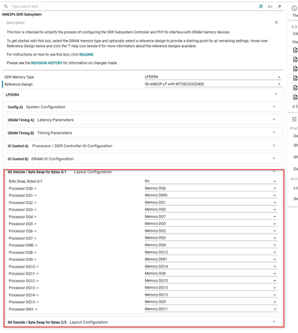
    Yes, software modification is absolutely necessary. Please use the DDR register configuration tool : dev.ti.com/.../ to modify the DDR configuration for your board. Check the README link in the tool for instructions. The DQ swapping definition can be changed in the tool:

    However, in below guideline, it mentions that sysconfig is "not necessary". If it is a typo?
    www.ti.com/.../sprad06c.pdf

    i did not realize you were taking about DDR4. Yes, for DDR4, it is not necessary to specify data swapping for normal DDR4 functional operation.

    https://e2e.ti.com/support/processors-group/processors/f/processors-forum/1313356/am625-ddr4-configuration?tisearch=e2e-sitesearch&keymatch=Am625%2520DDR4#

    In the sysconfig tool, for a 4GB DDR4 memory configuration:

    Which values of parameters do I need to change for System Configuration, Latency Parameters, and Timing Parameters?

    This would all depend on the memory you are using.  You would need to check all the timing parameters match the values in the DDR datasheet.  Latency and system configuration values would be determined by your system.  Ensure you also plug in the correct IO settings for termination and drive strength, these are dependent on your board design.

    The README link in the tool has some guidance on filling out each value for LPDDR4.  These instructions can be used as a guide for DDR4 as well.  DDR4 specific instruction will be coming soon to the tool

    AM625: DDR maximum size configuration in single chip select

    https://e2e.ti.com/support/processors-group/processors/f/processors-forum/1309940/am625-ddr-maximum-size-configuration-in-single-chip-select

    AM62x DDR4 supports max of 8GB with 2 ranks, 4GB with 1 rank
    LPDDR4 supports max of 4GB with 2 ranks, 2GB with 1 rank

    AM6442: Refresh Rate Setting of LPDDR4/DDR4 in PSDK Linux

    https://e2e.ti.com/support/processors-group/processors/f/processors-forum/1303237/am6442-refresh-rate-setting-of-lpddr4-ddr4-in-psdk-linux

    AM625: AM625:8bit,Single rank DDR4 chip x 2pcs support

    https://e2e.ti.com/support/processors-group/processors/f/processors-forum/1278830/am625-am625-8bit-single-rank-ddr4-chip-x-2pcs-support

    AM625: How to change device tree to incorporate DDR4 Data pin swaps

    https://e2e.ti.com/support/processors-group/processors/f/processors-forum/1276890/am625-how-to-change-device-tree-to-incorporate-ddr4-data-pin-swaps

    It should not be necessary to make any device tree changes on DDR4 to accommodate data bit swizzling.  What are you trying to read from DDR4?  What is PSCI?

    Good to know we don't need to change anything in device tree for DDR4 data pin swaps. 

    We are having issues with booting and I am trying to see what are the differences in our custom hardware when compare to eval board SK-AM62 and the Power State Coordination Interface (PSCI) is an ARM standard that describes a software interface for power management between an operating system is getting stuck when it tries to read the version number of the firmware.

    I wanted to rule out that this has nothing to do with DDR4.

    Using 2x LPDDR4 devices

    We currently only support one LPDDR4 device.  Trying to design with 2 LPDDR4 devices would require routing the data bus to two different devices, which we don't support. 

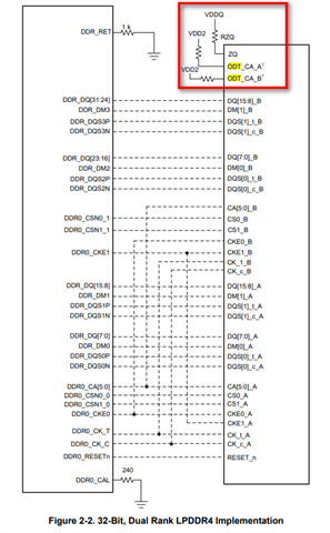
    The routing for dual rank would be the same as Fig 2-2 in the DDR layout appnote, with the addition of connecting CS1 and CKE1.

    AM625: 16bit DDR4 performance

    https://e2e.ti.com/support/processors-group/processors/f/processors-forum/1115076/am625-16bit-ddr4-performance/4669081

    The AM62x app report has been out for a while, see memory bandwidth and latency sections in https://www.ti.com/lit/pdf/sprad45 .

    AM625: DDR CLK termination specification

    https://e2e.ti.com/support/processors-group/processors/f/processors-forum/1231613/am625-ddr-clk-termination-specification/4665907

    This is actually taken from the DDR4 recommendation from Micron, in their appnote TN-40-40.  Here is the quote from the appnote:

    If simulations determine that AC termination is needed, terminate CK_t and CK_c through approximately 36Ω series resistors and a .01uF capacitor to VDD. A single approximately 36Ω resistor in parallel across CK_t and CK_c may also be adequate

    AM625: 2 DDR4 two, 4GByte total

    https://e2e.ti.com/support/processors-group/processors/f/processors-forum/1226452/am625-2-ddr4-two-4gbyte-total/4644834

    According to the design of the EVB board, the 16-bit DDR is also not VTT added, which appears to conflict with what is mentioned in sprad06.pdf. Which should be referenced? 

    The EVM has only one DDR4 device, which only presents one load on addr/ctrl signals.  Your design has 2 x8 devices and thus two loads, which would necessitate VTT termination because of the multiple loads.  We are in the process of adding this detail to the app note.  VTT-less design should only be used with one DDR device.

    AM625: Supported DDR4 SDRAM Combinations

    https://e2e.ti.com/support/processors-group/processors/f/processors-forum/1208607/am625-supported-ddr4-sdram-combinations/4588379

     2x MT40A4G8 can be supported.  Each device would be connected to each data byte.  The address/ctrl signals would be connected in fly-by topology with VTT termination.    I would recommend performing board level simulations to ensure proper signal integrity

    AM625-Q1: Is it possible to change the drive strength on AM625-q1 for DDR lines.

    for simulations, they have to change the model in order to choose a different driver setting.  The driver strengths can also be change for silicon using the DDR register configuration tool: https://dev.ti.com/sysconfig/?product=Processor_DDR_Config&device=AM62x

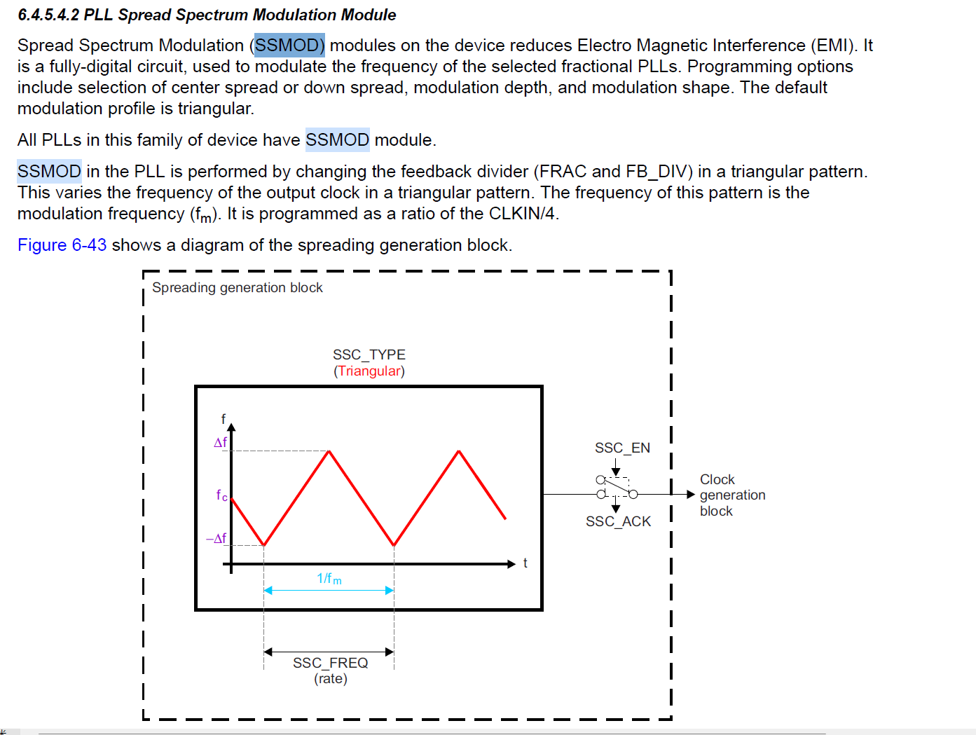
    AM625: external and internal spread spectrum oscillator support

    https://e2e.ti.com/support/processors-group/processors/f/processors-forum/1467752/am625-external-and-internal-spread-spectrum-oscillator-support

    AM625: LPDDR4 configuration and operating temperature

    https://e2e.ti.com/support/processors-group/processors/f/processors-forum/1234907/am625-lpddr4-configuration-and-operating-temperature

    So, for example, if you plan to operate all the way to 125C, change the Operating Temperature Range to -40C to 125C.  This also automatically de-rates some of the appropriate parameters (you can see these in the DDR datasheet)  (this answers your last question)

    You will also have to make the following changes manually in the tool

    tREFIab = 975ns

    tREFIpb = 122ns

    tRASmax = 8775ns

    tDQSCKmax = 3.6ns

    Note that the next release of the DDR register configuration tool (post v9.08) will make these changes automatically when you change Operating Temperature Range.  Once the SDK support dynamic changes, the config tool will change accordingly.

    DDR dynamic refresh feature is only available starting in Linux SDK 11.02.  It is not available in MCU+ SDK.

    (9) TDA4VM-Q1: TDA4VM-Q1 - Processors forum - Processors - TI E2E support forums

    https://software-dl.ti.com/jacinto7/esd/processor-sdk-linux-jacinto7/08_01_00_07/exports/docs/linux/Foundational_Components/U-Boot/UG-QSPI.html

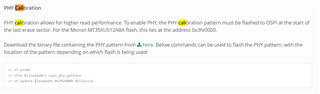
    Can you check the Phy calibration section:

    BTW if 08_00_00_08 is working well. Which is the failing release? Is it failing with latest 8.1 Release?

    Thanks for the pointers. we have tried as per above instructions but it didnt help in our custom board.

    also we have root caused the issue with DDR speed. we are using MT53D1024M32D4DT046 AUT:D chip in our design and speed we have set is 4266 MT/s. with the full speed we are facing power on OSPI boot issues. we have reduced the DDR speed to 3733 Mt/s and the issue is disaappeared in our custom TDA4Vm board. we are able to sucessfully boot the board without having any issues.

    could you please provide us some pointers how to do training of LPDDR4x memory to support 4266MT/s with our custom board.

    Can you please try the following manual changes to your DTSI file?

    • For below registers, change the '7' to a '6' as shown below

    #define DDRSS_PHY_33_DATA 0x0C002006
    #define DDRSS_PHY_289_DATA 0x0C002006
    #define DDRSS_PHY_545_DATA 0x0C002006
    #define DDRSS_PHY_801_DATA 0x0C002006

    • For below registers, change the '20' to a '40' as shown below

    #define DDRSS_PHY_32_DATA 0x10400000
    #define DDRSS_PHY_288_DATA 0x10400000
    #define DDRSS_PHY_544_DATA 0x10400000
    #define DDRSS_PHY_800_DATA 0x10400000

    AM623: Operating temperature range at DDR config

    https://e2e.ti.com/support/processors-group/processors/f/processors-forum/1266719/am623-operating-temperature-range-at-ddr-config/4805779

    we are in a bit of a transitional period to help support the range of temps supported by DDR. 

    First for LPDDR4, i believe the v9.1 of the SDK (not released yet) will support dynamic changes (ie, temperature controlled refresh mode).  Currently, you have to choose the highest temperature you plan to operate, and configure the DDR Register Configuration Tool for that temperature.  The latest version of the tool v9.09 will automatically change the appropriate parameters when the temp setting is changed in the tool.  You will see these values change in the tool as you change the temp setting.   Since dynamic refresh rate changes aren't support yet, the tool will simply configure the refresh rate to 4x to support the higher temps.  It will also derate some of the other timings automatically, so all you should need to do is set the temp in the tool appropriately (there appears to be some typos in the README related to this, which will get fixed in the next release)

    For DDR4, it is a different story.  DDR4 doesn't have the same temp refresh mode as LPDDR4, so this is not relevant for software to support.  In the tool, you would choose the appropriate temp range for your design, and this will change MR2[7:6]= 11b to support auto self refresh mode.  MR4[3:2]  will also be changed to 11b to support temperature controlled refresh.  tREFI, tRFC, and tRAS do not automatically change, so this will need to be done by the user.  A future version of the tool will auto change the refresh rate to facilitate this.

    (12) AM625-Q1: When using the AM625, executing commands may cause system crashes. - Processors forum - Processors - TI E2E support forums

    AM625-Q1: When using the AM625, executing commands may cause system crashes.

    we identified that they're actually use a 512MB ddr4l memory on board but not configure the uboot and kernel memory size correctly within both sites of dts, to reflect 512MB judge from the logs they provided and customer's schematic design.

    To configure DDR size in U-Boot, it is in the same memory@800000000 node, but in U-Boot file dts/upstream/src/arm64/ti/k3-am625-sk.dts.

    Specifically for 512MB DDR, you would also need to add

    CONFIG_SYS_MEM_TOP_HIDE=0x02500000

    to U-Boot file configs/am62x_evm_r5_defconfig and cofigs/am62x_evm_a53_defconfig.

    Miscellaneous

    https://e2e.ti.com/support/processors-group/processors/f/processors-forum/1337414/am625-am625/5138084

    https://e2e.ti.com/support/processors-group/processors/f/processors-forum/1310813/am625-on-package-and-ondie-decoupling/4997031

    https://e2e.ti.com/support/processors-group/processors/f/processors-forum/1290613/am625-jtag-unlocking-via-secure-access-point-with-lauterbach/4904471

    https://e2e.ti.com/support/processors-group/processors/f/processors-forum/1276325/am625-please-help-confirm-whether-ddr4-and-emmc-can-be-supported

    https://e2e.ti.com/support/processors-group/processors/f/processors-forum/1266441/sk-am62b-deep-sleep-demo-on-am62b

    https://e2e.ti.com/support/processors-group/processors/f/processors-forum/1432193/am62p-how-to-design-am625-am62p-with-lower-power-consumption/5492392

    https://e2e.ti.com/support/processors-group/processors/f/processors-forum/1204192/am625-lpddr4-spacing-requirements

    https://e2e.ti.com/support/processors-group/processors/f/processors-forum/1252323/am625-overshoot-and-undershoot-voltage-measurement-for-lpddr4

    https://e2e.ti.com/support/processors-group/processors/f/processors-forum/1137904/am625-lpddr4-product-selection

    The AM62x has been validated with Micron  MT53E2G32D4DE-046.  The SDK will support the device on the AM62x Low Power EVM, which has a similar device MT53E1G16D1FW-046.  The design files for this board have not been released yet

    (+) AM64x - Queries related to memory devices selection - Processors forum - Processors - TI E2E support forums

    Sl No

    Interface/Description

    Part Number

    Alternate Part number

    1

    LPDDR4-4Gb, 200-ball, 3200Mbps

    W66CP6RBQAFJ

    MT53E256M16D1FW-046 AAT:B

    The Winbond LPDDR4 looks to be compatible from a datasheet standpoint.  Please ensure proper board design guidelines are met: https://www.ti.com/lit/pdf/spracu1

    (3) AM620-Q1: LPDDR INTERFACE - Processors forum - Processors - TI E2E support forums

    For the AM625 / AM623 Starter Kit (EVM) with (AM6204BTGFHIALWRQ1), we have customized the design according to our requirements and replaced the LPDDR with IS46LQ16512B-053BLA1. We would like to know how to confirm the feasibility and compatibility of this change with the processor. We have also attached the datasheet for your reference.LPDDR46LQ16512B (1).pdf 

    Please use the AM62x DDR Register Configuration tool: https://dev.ti.com/sysconfig/?product=Processor_DDR_Config&device=AM62x to configure the ISSI LPDDR4 (instructions are in README in the tool).  This tool will generate a header file which needs to be built into your code so the driver can initialize the DDR appropriately.  For functional validation, i would recommend using linux memtester or other memory stress tool and run across your expected operating temperature range.

    https://e2e.ti.com/support/processors-group/processors/f/processors-forum/1169192/am625-lpddr4-logic-compatibility-with-am625x

    The processor conforms to the JEDEC LPDDR4 spec, so you should be able to get the information you are looking for from that spec. 

    The AM62x is JEDEC compatible to the LPDDR4 spec.

    Kindly let us know the JEDEC standard number your referring to. We need this information to cross verify with the lpddr4 part.

    it is LPDDR4 JESD209-4B

    https://e2e.ti.com/support/processors-group/processors/f/processors-forum/1234595/am625-how-to-measure-lpddr4-clock

    Can we perform Signal integrity validation check on the DDR clock probed on the vias without causing any loading effect due to the probe.? kindly let us know.

    Yes, typically you would need to use high speed active FET probes

    Would it be possible to monitor the lpddr4 signals through JTAG? Can the lpddr clock frequency be measured through JTAG? Can the lpddr4 timing parameters like setup,holdtime be validated through JTAG? We have the XDS110 JTAG debugger from TI .pls let us know if we can use this debugger to monitor the lpddr4 signals.

    No, JTAG is just used for debugging code or in some instances for code trace capabilities. There is no way to measure signals using JTAG.

    [FAQ] AM623: LPDDR4 Padstack size

    https://e2e.ti.com/support/processors-group/processors/f/processors-forum/1356111/faq-am623-lpddr4-padstack-size


    PCB pad is NSMD and LPDDR4 package pad is SMD, so the PCB pad should be smaller than the Ø0.40 SMD opening on LPDDR4 package. The ratio is 1:0.8 (Pkg SMO: PCB pad)
    With NSMD, the pad can be smaller as solder wets the sides/wall of the pad.
    Note that the raw ball size is Ø0.436mm according to Micron datasheet.

    Refer to https://www.micron.com/content/dam/micron/global/public/products/customer-service-note/csn33-bga-user-guide.pdf
    * Table 3: Examples of Recommended PCB and Package Interconnect Opening Dimensions
    * Printed Circuit Board Design Guidelines (pros and cons)
        - NSMD pads are smaller and offer more space for trace routing than SMD pads
        - SMD solder joints have higher standoff, which makes the joints more robust during shock or drop events

    Consider Board Level Reliability Testing for your end product

    Refer also to IPC publication 7351 Generic Requirements for Surface Mount Design and Land Patterns

    https://e2e.ti.com/support/processors-group/processors/f/processors-forum/1246018/am625-if-ddrss-connect-2-x-2gb-ddr4-processor-can-see-as-4gb-ddr4/4725439

    You have to ensure to maintain only 1 load on each of the data bytes.  You cannot connect devices in parallel where the data bus would be split on the board.

    You can use something like Micron's MT40A4G8 and use 2 ranks to achieve up to 8GB, or you can use the single rank MT40A2G16 to achieve 4GB

    Software patches to achieve 4GB can be found in this thread: https://e2e.ti.com/support/processors-group/processors/f/processors-forum/1235702/am623-memory-can-t-be-configured-to-4gb-from-device-tree/4681818#4681818

    https://e2e.ti.com/support/processors-group/processors/f/processors-forum/1247698/am625-ddr4-si-signal-integrity-testing

    we don't have a tool for this type analysis at this time.  I would suggest to perform high stress memory tests to prove out your board design.  We typically use linux memtester at your max operating frequency, and across temperature if possible, to ensure a stable interface.

    https://e2e.ti.com/support/processors-group/processors/f/processors-forum/1242377/am625-external-ram-supported-by-am62x-family/4697329

    AM62x only supports DDR4 and LPDDR4 devices. Please refer to the datasheet for max frequency/size specifications. 

    You can refer to our SK-AM62 for a recommended DDR4 implementation using  MT40A1G16KD-062E IT:E. This page should have all design documents which may simplify a customer design: https://www.ti.com/tool/SK-AM62 

    I would also recommend the customer review the DDR Board Design app note for any additional information on how to design a successful system: https://www.ti.com/lit/pdf/sprad06 

    https://e2e.ti.com/support/processors-group/processors/f/processors-forum/1207903/am625-sdk-08-06-00-42-kernel-5-10-gpio-state-on-deep-sleep/4557231

     AM625: Memory read latency problem 

    https://e2e.ti.com/support/processors-group/processors/f/processors-forum/1196156/am625-am6254atgghaalw

    The DDR4 I/O model is contained within the IBIS model for AM62x which is available on ti.com. No separate controller timing model is required for SI simulations.

    https://e2e.ti.com/support/processors-group/processors/f/processors-forum/1172501/am625-ddr-cke-pin/4413351

    ok this will occur during a power down sequence as show in figure 7-6 of the datasheet.  Note that the first thing is MCU_PORz activating low, this will put the DDR subsystem in reset (and thus the DDR PHY) and tri-state all DDR signals.  If they want to ensure CKE low, they would need a pull down on the signal.

    I think the original question implied they were intending to keep the processor alive and just power down the LPDDR4, which i wouldn't recommend.

    https://e2e.ti.com/support/processors-group/processors/f/processors-forum/1164215/am625-ddr4-layout-impedance

    According to our experts, 50ohm DDR trace impedance will result in impedance mismatches in the system.  The customer can design a board with 50ohm impedances, but they must run simulations for data read/write and addr/ctrl to ensure proper signal integrity.  

     AM625: in-line ECC support 

     the inline ECC feature should be available with any memory.  I don't see a reason why it would not work.  Note that i don't know the extent of software support for DDR ECC.  It does take some configuration which i'm not sure is supported by the driver yet.

    https://e2e.ti.com/support/processors-group/processors/f/processors-forum/1402986/am625-how-to-set-correct-vdd_core-vdda_ddr_pll0-for-lpddr4/5378950

    https://e2e.ti.com/support/processors-group/processors/f/processors-forum/1353838/am625-am625-transient-overshoot-and-undershoot-at-io-pins/5162316

    AM625: LPDDR4 configuration - how to configure IO configurations?

    I helped the customer configure the timing parameters for this memory (attached syscfg).

    However, I am unsure of how to configure the IO configurations and what they mean for the system and where to look for this info. Can you suggest me what the right configurations should be for this LPDDR4? In general, what resources should be followed to do this configuration?


    IO configurations are usually taken from board simulations. Typically different values of drive strength and termination can be simulated to determine which setting provide the widest data eyes.

    https://e2e.ti.com/support/processors-group/processors/f/processors-forum/1129776/am625-running-cpu-s-at-1-4ghz-with-tps6521902-and-lpddr4

    We need to understand if there is a valid procedure for first increasing the PMIC voltage (TPS651902 buck 1) and then boosting the A53SS to 1.4GHz post reset (during boot). You have not answered this question, and we require an answer so that the customer can move forward with their design.

    AM62x doesn't support dynamic voltage scaling, so the PMIC can only be programmed to a fixed voltage to support AM62x.

    https://e2e.ti.com/support/processors-group/processors/f/processors-forum/1265418/am625-q1-low-power-numbers/4800140

    https://e2e.ti.com/support/processors-group/processors/f/processors-forum/1229290/am6411-ddr-bandwidth-in-case-of-multi-core-running-with-both-a-core-r-core/4661165

    I am not aware of the kind of DDR benchmarking you are asking about - we will have to see if the current thread assignee has any other input.

    This discussion on another e2e thread about setting DDR access priority might be of interest to you:
    https://e2e.ti.com/support/processors-group/processors/f/processors-forum/1220944/am625-lpddr4-access-priority

    The M4F does have access to DDR memory, like the other cores. Please keep in mind that the M4F is different from the R5F cores, in that M4F does not have local cache memory. That means that each M4F access to data stored in DDR memory will take the full read time for the signal to travel out of the M4F, across the device, to the DDR, and back. At least on AM62x, we have measured M4F reads to DDR memory taking about 100 M4F clock cycles. Reference this FAQ for more information: https://e2e.ti.com/support/processors-group/processors/f/processors-forum/1187962/faq-sk-am62-how-to-execute-code-from-external-memory-using-m4f-core

    Regards,

    Sreenivasa

  • Hi Board designers, 

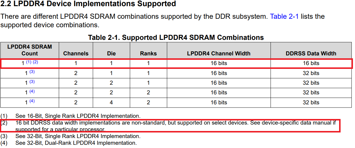
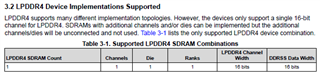
    Could you please confirm if the AM62A74AUMSIAMBRQ1 MPU supports a 16-bit single-channel LPDDR4 configuration, as shown in the attached image?

    We have reviewed the TI documentation but haven't found an explicit statement confirming whether this specific mode is supported.


     Also can we use 2 physical 16bit LPDDR4 chips to fill whole 32bit bus?

    Yes, the AM62A74AUMSIAMBRQ1 explicitly supports a 16-bit single-channel LPDDR4 configuration. Multiple TI documents confirm this for the AM62A family, and dedicated design guidelines exist for this exact topology.

    Also, two physical LPDDR4 devices is not allowed.  This would require DQ bus to be split on the board, which is not allowed.

    Supported Memory Configurations

    The AM62A7 DDR subsystem (DDRSS0) supports exactly two allowed configurations [1]:

    Configuration
    Supported?
    1× 32-bit (standard dual-channel)
    White check mark Yes
    1× 16-bit (single-channel)
    White check mark Yes
    1× 8-bit
    X Not allowed

    The AM62A7-Q1 Hardware Design Guide further confirms that DDRSS0 supports interfacing with 16-bit or 32-bit SDRAM, with LPDDR4 as the supported memory interface type [2].

    "Non-standard" does not mean unsupported. TI describes 16-bit implementations as non-standard relative to the typical 32-bit dual-channel LPDDR4 topology, but explicitly states they are supported on select devices — and the AM62A family is one of them [3]. A dedicated application note, SPRAD66B, even includes Figure 2-3: 16-Bit, Single Rank LPDDR4 Implementation with full board design and layout guidance [3].

    Implementation Requirements

    If you proceed with this configuration, note the following mandatory design considerations:

    • Point-to-point topology is required for the data bus in 16-bit configurations — T-branching or fly-by is not allowed for data signals [5].  
    • T-branching is required for CA lines in all LPDDR4 designs; fly-by topology is not permitted [6].  This only applies when using a dual channel device and utilizing both channels.
    • Unused signal handling: Specific guidelines apply for unused signals such as DQS2 and DQS3 when operating in 16-bit mode — these must be properly terminated per the 16-bit single-rank implementation guidelines [1]
    • Maximum capacity: Single-channel, single-rank LPDDR4 supports up to 2GB [6]
    • U-Boot/software configuration: The DDR configuration in U-Boot must be adapted to match your specific LPDDR4 memory part and 16-bit hardware implementation on your custom board [7]

    Citations

    1. AM62Ax DDR Board Design and Layout Guidelines (SPRAD85D)
    2. AM62A7-Q1 Hardware Design Guide (SPRADO2C)
    3. AM62Ax LPDDR4 Board Design and Layout Guidelines (SPRAD66B)
    4. AM62Ax/AM62Px General Layout Guidelines (SPRAD21I)
    5. E2E FAQ: AM62Ax Common Design Errors – DDR/LPDDR4 Memory Interface
    6. E2E FAQ: AM62Ax Board Layout Links and High-Speed Layout Guidelines
    7. E2E: AM62A7-Q1 U-Boot DDR Configuration for Custom Hardware

    e2e.ti.com/.../am62p-q1-dqs-connection-between-am62p-and-lpddr4

    No, differential signals cannot be swapped.  You can only swizzle DQ or DM within a byte.  Please refer to layout guidelines: https://www.ti.com/lit/pdf/sprad66

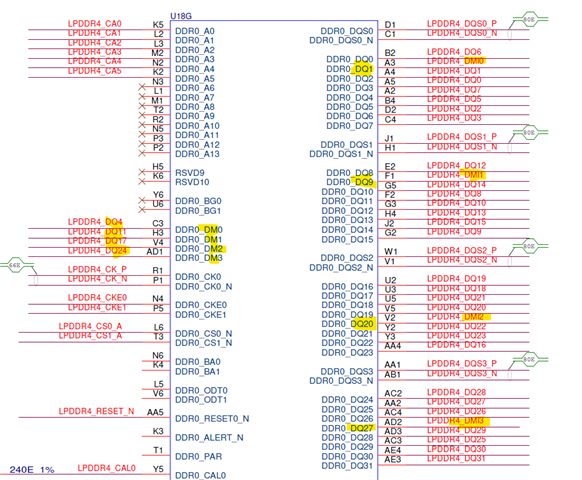
    Based on the reference design (SK-AM62P-LP, SPRR487C, PROC164E2). I have some questions regarding the LPDDR4 interface:

    1. Data pin swapping: Not only are data lines swapped within a byte, but the DataMask (DM) lines are swapped as well. Is this possible because the assignment per byte (DQ & DM) can be configured individually?
    2. CLK impedance: I also noticed that the CLK signal is routed with an impedance of only differential 66 ohm. What is the reason for this impedance value?


    yes, DQ and DM signals within a byte can be swizzled.  This can be defined in the DDR register configuration tool:

    For the CLK impedance, this is what we specify in the DDR Layout Guidelines: https://www.ti.com/lit/pdf/sprad66

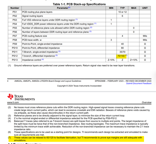
    Also see note 5, which explains that since the CLK and address signals have to be T-branched on board, the impedance should be div-by-2 for the branched portion of the trace.

    Single rank LPDDR4 interface for AM62A, AM62D-Q1, AM62P

     W66CP2NQQAFK is a single rank device, they should be referring to Figure 2-1 32-Bit, Single-Rank LPDDR4 Implementation in the app note.  You can see from the diagram that address/control signals need to be T-branched on the board to connect to both channel A and B

    (+) AM62P: the guideline of LPDDR4 simulation - Processors forum - Processors - TI E2E support forums

    Since memories only have one setting for CA/CS, we choose 80ohm.  Then since CS is point to point, CS driver is set to 80ohm.  Since CA signals are T-branched, CA driver is set to 40ohm, and because of the T-branch, each branch would then be 80ohm.  This combination provides the best chance for impedance matching.

    The controller has separate driver control for CS and CA.  As was done in the AM62Px configuration, i think you should keep CA 40ohm driver, CS 80ohm driver.  And then in the memory, you can choose 80ohm termination.  With the split CA bus, this would be the best way to match impedances.  What is the trace impedance on your board?

    ODT configuration:

    The configuration tool is used to configure the DDR controller and PHY and set it up so the hardware can correctly perform initialization and training to get it ready for normal operation
    Regarding the LPDDR4 initialization, we try to simplify the process by providing specific layout guidelines and a sysconfig tool which facilitates DDR register configuration for custom boards. This helps to abstract most of the details of configuration the DDR controller and PHY. The ddr software driver in our SDK will consume this register configuration header file and perform the necessary steps for initialization.

    Output impedance and ODT settings are typically determined through SI board simulations. The ones you point to in the RegConfig tool are optimized for the TI SK EVM. ODT and output impedance are set in the tool
    Processor side (under IO Control A):
    -"Driver pull up/down" sets the output impedance for DQ or CA (set the pull up and down to the same value)
    -ODT Pull Down sets ODT for DQ (only pull down is set for LPDDR4)
    DDR side (under IO Control B)
    -"Drive Strength Pull_down" sets the output impedance for DQ
    -"Termination CA ODT" or "Termination DQ ODT" sets the ODT in the memory for cmd/addr and data respectively

    Could you tell me the DDR register setting below?
    Termination: CA ODT
    Termination: DQ ODT
    VREF Control: DQ VREF
    VREF Control: CA VREF
    Driver Pull-Up Lane 0/1 DQ/DM
    Driver Pull-Down Lane 0/1 DQ/DM
    Driver Pull-Down CA[5:0]
    Driver Pull-Down CA[5:0]
    We need them to evaluate DDR.
    these values are all based on the board design, and ideally should be provided as a result of power aware board simulations.

    Is dynamic ODT recommended over static ODT, if the nominal ODT is RZQ/4 or RZQ/2? I am assuming these dynamic values are spec'ed by the DDR vendor ...
    There are 2 different ODT settings on the DRAM. The Rtt_Nom (your reference to Static ODT) and Rtt_WR (dynamic ODT). Rtt_Nom if enabled, is used to terminate the Data lines during idle conditions and during Write operations if Rtt_WR (dynamic ODT) is not set. Rtt_WR is only set during WRITE operation. If Rtt_WR is set along with Rtt_Nom then the memory switches the ODT setting from Rtt_Nom to Rtt_WR value dynamically. The best setting is ideally derived by performing signal integrity simulations. In general, I would suggest that for lower power operation, it is preferable to just set the Rtt_WR (or) dynamic ODT and not enable the Rtt_Nom. For best signal integrity, Rtt_Nom should be set to a low value (RZQ/6 or RZQ/12) and Rtt_WR can be set to either RZQ/4 or RZQ/2. All of these ODT values are part of the DRAM specification

    Is dynamic truly mutually exclusive to static ODT, i.e. the static settings in DDR_TERM have no effect, if DYN_ODT is set?
    They are mutually exclusive in the sense that you can enable them independently. However, if you set the DYN_ODT i.e. Rtt_WR to a different value from Rtt_Nom, the ODT value will change for WRITE operation as set in Rtt_WR

     AM620-Q1: LPDDR INTERFACE 

    Please use the AM62x DDR Register Configuration tool: dev.ti.com/.../ to configure the ISSI LPDDR4 (instructions are in README in the tool). This tool will generate a header file which needs to be built into your code so the driver can initialize the DDR appropriately. For functional validation, i would recommend using linux memtester or other memory stress tool and run across your expected operating temperature range.


    RE: AM623: LPDDR4 ODT Configuration options 

    You can look in the DDR Register Config tool for AM623: https://dev.ti.com/sysconfig/?product=Processor_DDR_Config&device=AM62x

    Section IOControlA has drive and termination settings for the processor. Section IOControlB has drive and termination settings for the memory. Check the README in the tool for more details


    RE: AM62A7-Q1: CA and CS ODT of DDR 

    LPDDR4 memories do not allow for separate CA/CS termination settings. With MR22, you can selectively enable/disable the ODT. Check your DDR datasheet or JEDEC spec for more info.

    We do allow independent configuration of CA and CS drive strength in the processor (see excerpt below from DDR Register Configuration Tool). Note that all these settings for a custom board should be configured with the DDR Register Configuration tool

    dev.ti.com/.../

    RE: AM623: How do I set the DDR4 register? 

    here's an explanation of the changes that need to be made in the IOControlA and IOControlB sections in the tool:

    IOControlA
    Clock ddr4_ocd_48p_48n_diff: this is the clock driver of AM623, simulation model used was 48ohm differential impedance.
    Address, Command ddr4_ocd_48p_48n: similary, this is the addr/cmd driver of AM623, 48ohm impedance model was used.
    In the tool, this corresponds to "Driver Impedance for Addr/Ctrl/Clk = 48ohm
    =================================
    Data ddr4_ocd_48p_48n: this is the data driver for AM623, simulation model used 48ohm impedance
    Data Mask ddr4_ocd_48p_48n: this is the DM driver for AM623, simulation model used 48ohm impedance
    Data Strobe ddr4_ocd_48p_48n_diff: this is the DQS driver for AM623, simulation model used 48ohm diff impedanc
    In the tool, all 3 of these correspond to "Driver Impedance for DQ/DQS/DM" = 48ohm
    =================================
    CPU ODT (READ) is the termination in AM623 for the read data. This shows 60ohm.
    In the tool, this corresponds to "ODT for DQ/DQS/DM" = 60ohm
    =================================
    IOControlB
    DDR4 Output Impedance (READ) is the data driver for the memory. This shows 48ohm in the last column
    In the tool, this corresponds to Output Driver Impedance (ODI) = 48ohm
    =================================
    DDR4 ODT(WRITE) is the termination in the memory for write data. This shows 60ohm
    In the tool, this corresponds to "Nominal ODT (RttNOM)" = 60ohm
    The rest of the parameters in IOControlA and IOControlB can be left as default

    e2e.ti.com/.../5112160
    The ODT values for both processor and memory can be set using the DDR register configuration tool. The values follow what is spec'ed in the JEDEC spec. IO calibration is automatically enabled on the processor side, and can be enabled on the memory side. This calibration adjusts the output driver impedance of the IOs and can be enabled periodically to perform the calibration dynamically.

    e2e.ti.com/.../4433869
    the default values in sysconfig for DDR4 will work for the AM64x EVM. The configuration from the SDK that you started with may be slightly different, but that is just because the sysconfig tool has been updated since that configuration was generated. I would start with the latest output from the sysconfig tool with the default DDR4 values, just to make sure you are at a same working starting point. Then start making your adjustments.

    e2e.ti.com/.../6390061
    it shows 40ohm driver and 80ohm ODT for both read and write, but you don't have that set up in the DDR configuration file.
    However, i've never seen 80ohm ODT for this configuration. Can you try changing all processor DQ ODT to 40ohm by changing the following in the DDR configuration tool
    Termination: DQ ODT (FSP2) = RZQ/6(40ohm)
    Termination: SOC ODT (FSP2) = RZQ/6(40ohm)

    JacintoTm 7 DDRSS Register Configuration Tool
    https://www.ti.com/lit/an/spracu8b/spracu8b.pdf

     RE: TDA4VH-Q1: Choosing the correct ODT-models from IBIS file for LPDDR interface signal integrity analysis 

    Below are the defaults settings for the TDA4VH EVM.

    Processor Side
    DQ / DQS Drive Strength (WRITEs): 40 ohms
    DQ / DQS ODT (READs): 40 ohms
    CA / CK Drive Strength: 40 ohms
    CS Drive Strength: 80 ohms
    DRAM Side
    DQ / DQS Drive Strength, or PDDS (READs): RZQ/6 (40 ohms)
    DQ / DQS ODT (WRITEs): RZQ/5 (48 ohms)
    CA/CK/CS ODT: RZQ/3 (80 ohms)

    e2e.ti.com/.../6113314
    Termination

    The DDR clock is terminated by the LPDDR4 memory.
    LPDDR4 memory does not have a dedicated ODT configuration for DDR clock. Rather, the CK ODT configuration is shared with the CA and CS signals, and defined by MR11[6:4].
    MR11[6:4] is configured by the input "Termination: CA ODT" under the "IO Control B) DRAM IO Configuration" setting.
    Drive Impedance
    The AM67 DDR register configuration tool does not have a unique DDR clock drive impedance configuration input.
    The DDR clock drive impedance configuration will be set based on the CA drive impedance configuration (parameter "Drive Strength: CA[5:0]" under section "IO Control A) Processor / DDR Controller IO Configuration").


    RE: TDA4VE-Q1: LPDDR4 design guide what the exact value for the pull up res of ODT? 

    The specific resistor value is not critical - as its not a calibration or termination resistor value. It is a logic input - so any resistor value can be used as long as it sets the correct logic value. All the resistor values you mentioned (10K, 2.2K, 1K) should all be fine.

     AM67: LPDDR4 ODT termination 

     RE: AM68A: LPDDR4 Impedance and ODI/ODT termination (SK-AM68) 

    Yes data groups and address/control groups have separate settings for ODI/ODT.

    Does spracu8b include settings for TDA4-VE EVM? Same settings used for SK-AM68.

    Regarding stub lengths - recommend simulation determine how the stub length impact your design performance. We have provided some stub length recommendations in the LPDDR4 Design Guidelines application note.

    (+) TDA4VEN-Q1: LPDDR4 IF ODT_CA connection for J722S - Processors forum - Processors - TI E2E support forums

    The pull-down resistors should not be installed.  The ODT_CA signals should be pulled-up to 1.1V.

    Regards,

    Sreenivasa

  • Hi Board designers, 

    Pins not supported on AM62L for DDR interface compared to AM62x

    The DDRSS does not support DDR0_ALERT_n, DDR0_PAR, DDR0_CKE1, DDR0_CS1_n, DDR0_ODT1 signals (pins). It is recommended to follow the memory data sheet recommendations  or consult memory supplier to connect any of the available signals   that are not interfaced to the processor DDRSS

    Connection recommendations:

    TN-40-40: DDR4 Point-to-Point Design Guide Pin Connection Guidance page 29

    (+) AM62L: AM62L31:designing with DDR4, how should the related pins be handled? - Processors forum - Processors - TI E2E support forums

    This app note from Micron mentions that both can be left floating if not used: https://www.mouser.com/pdfDocs/Micron_DDR4_Design_Guide.pdf?srsltid=AfmBOopPVSeVWkCJ_gfRvpDHrEDBM36-T5-VOMgrKrhOfsrwqK4HvREO

    Regards,

    Sreenivasa

  • Hi Board designers, 

    SK / EVM references for AM62L DDRSS interface

    TMDS62LEVM AM62L evaluation module

    https://www.ti.com/tool/TMDS62LEVM

    The AM62L evaluation module currently supports LPDDR4 interface 

    SK-AM62B-P1 AM62x Starter Kit EVM with PMIC

    https://www.ti.com/tool/SK-AM62B-P1 

    The SK supports DDR4

    TMDS64EVM AM64x evaluation module for Sitara processors

    https://www.ti.com/tool/TMDS64EVM

    The EVM supports DDR4 with VTT terminations

    SK-AM62-LP AM62x starter kit for low-power Sitara processors

    https://www.ti.com/tool/SK-AM62-LP

    The SK supports LPDDR4 interface

    https://www.ti.com/tool/SK-AM64B 

    SK-AM64B AM64B starter kit for AM64x SitaraTm processors

    The SK supports LPDDR4 interface

    Note: AM62L DDRSS IP is similar with reduced addressable range.

    Regards,

    Sreenivasa

  • Hi Board designers, 

    Information related to DDR4connection of LDO  VTTSNS

    https://www.ti.com/lit/ds/symlink/tps51206.pdf

    VTTSNS Connection

    Figure 25. R-C Filter for VTTSNS

    Regards,

    Sreenivasa

  • Hi Board designers, 

    DDRSS related queries recently supported

    Our customer is using AM6412 with DDR4.  They're having a very hard time with lead times right now, and being told they need to move on to DDR5, which unfortunately would mean they move on from AM6412.  Can you review the list below, and let me know if it's possible their problems can be solved by changing to different DDR4 devices or a different class of memory that works with AM6412 (LPDDR4?).

    Kingston

    D5116AN9CXGXN

    Micron

    MT40A512M16TB-062E:R

    Nanya

    NT5AD512M16C4-JR

     all 3 of those are good alternatives. They have all been used in the past by other customers or have been used on our internal boards successfully

    They should be able to get alternatives from other vendors such as ISSI, Winbond, Samsung, Alliance.  Most vendors will supply JEDEC compliant devices, so they should be able to find compatible devices.

    If they can re-design to LPDDR4, these same vendors would also be good sources for those as well.  

    Our understanding is that vendors will still supply DDR4/LP4 well into the future for industrial customers.

    e2e.ti.com/.../am6442-lpddr4-32-bit-on-am64
    My customer is currently using 2GB LPDDR4 on AM64.
    However, as there is a shortage on those memories nowadays they wanted to check if it is possible to leverage a 32-bit LPDDR4 by only connecting 1x16b channel to this.
    In my understanding this should be possible but they would loose 50% of the total LPDDR4 memory. Is this assumption correct?
    this is correct. They can leave the upper 16-bit unconnected, and only be able to access half the memory


    AM62P- We are currently considering a change to LPDDR4 SRAM. Changing from a single die to two dies will double the current consumption of the LPDDR4 SRAM. Will this affect the SoC?
    Since the ports visible to the SoC remain unchanged, I believe the current consumption will not change, but I am checking just to be sure.
    The part numbers are as follows:
    Before change: MT53E512M32D1ZW-046 AAT:B
    After change: MT53E256M32D2FW-046 AAT:B(Z00M)
    The current consumption of the LPDDR4 may change, but you will have to check the LPDDR4 datasheet for those numbers. From the SOC point of view, the current consumption should be similar with a one or two die memory.

    1st DDR was MT53E1G32D2FW-046 AAT:B and you commented the 2nd DDR will be MT53E1G32D2FW-046 AIT:A,
    which means the difference between those two is only 'Operating Temperature':
    MT53E1G32D2FW-046 AAT:B (-40C to +105C)
    MT53E1G32D2FW-046 AIT:A (-40C to +95C)
    Then I think there will be no differences in DDR parameters and you can use the same configuration for those two devices.

    We use AM62D and AM62P and have been in an ongoing effort to source alternative DDR4 chips that are compatible with Micron MT53E128M32D2DS-046 AUT:A
    To that end, they had the following questions on 2 chips they found:
    We found supply from Alliance but with a slower clock of 1600Mhz. Is there anything here that would be a show-stopper? Our memory used lowest clock is at 1866Mhz.
    Also, there are Micron MT53E512M32D1ZW-046 AAT:B available but with a different die layout that might require a different memory controller or other changes. Is this viable?
    Any red flags? Your inputs are much appreciated to help save them time on validating memories.
    As far as Alliance memories go, we have had other customers successfully use Alliance memory with Sitara processors. If the memory is rated for 1600MHz, then you would have to configure the AM62D/P for the 1600MHz interface and could not go higher. You may also need to tweak some IO parameters (termination and drive strength), but otherwise you should be able to come up with a software DDR configuration that works.
    The different die layout shoudn't be too much of a problem. This is actually the same device we use on some of our EVMs, so this device has been fully validated with Sitara processors.

    e2e.ti.com/.../am6442-am6442-lpddr4-parts-support
    AM64x DDR interface is compatible with any LPDDR4 devices that are JESD209-4B standard-compliant. We have seen many customers use ISSI LPDDR4 memories successfully with AM64x and other Sitara processors. We have not done any specific validation with the part you quote, but it appears to be compatible.

    e2e.ti.com/.../6369714
    Alternative vendors include Nanya, ISSI, Winbond, Samsung, Hynix, Kingston, Alliance, among others. Since most DDR4 are JEDEC compatible, BGA footprint should be compatible.

    e2e.ti.com/.../6364745

    e2e.ti.com/.../6362678
    e2e.ti.com/.../6362557
    LPDDR4 devices that are compliant to JESD209-4B or later are compatible to AM64x devices. There may be new features described in JESD209-4C and future versions that are not supported, only the features described in the 4B version are supported.
    e2e.ti.com/.../6361490
    Can below 2 devices be used with AM625-Q1
    MT53E256M32D2DS-046 AAT:B
    MTFC32GBCAQDQ-AAT
    The DDR device can be used, but it is a dual channel device. You would only be able to use a single channel, and thus only half of the memory will be accessible. The eMMC device also can be used.

    e2e.ti.com/.../6353450
    you can use a dual-channel memory, but realize you will only be able to connect one channel to AM24x, which means that you would only be able to access half of the total memory density. The other half would not be accessible. So you would have to have a memory that is twice the density of the memory you need for your application.
    e2e.ti.com/.../6353435
    This app note from Micron mentions that both can be left floating if not used: www.mouser.com/.../Micron_DDR4_Design_Guide.pdf
    e2e.ti.com/.../6345635
    e2e.ti.com/.../6340188
    This configuration, which is supported, just connects a single channel of a dual channel device. So half the memory will be wasted, as you would not be able to access Channel B.
    e2e.ti.com/.../6304531
    e2e.ti.com/.../6291857
    e2e.ti.com/.../6279913
    we have not specifically validated Kingston or ISSI memories, but both have been successfully used in customers designs. Ensure board design guidelines are followed: www.ti.com/.../spracu1
    and generate a new DDR configuration for your board using the DDR register configuration tool: dev.ti.com/.../ (instructions are in the README link in the tool)
    e2e.ti.com/.../6276635
    1. Yes, use the DDR Register Configuration tool to generate a new configuration. For two x8 devices, you would change the Data Bus Width = 8, and Density per device (in your case to 8Gb per device). Ensure single or dual rank is selected as appropriate. Generally, most timing parameters will stay the same, but i would double check each one with the spec. Parameters like tRFC may change with density differences. IO parameters like drive strength or termination may also need to change. You would need perform simulation again to obtain optimal values for the new board design.
    2. You can follow the layout guidelines here: www.ti.com/.../sprad06. Fly-by topology is required for multi-package designs, and VTT is also required for multi-package board designs, as shown in the app note
    3. Yes, you should perform simulations since the board topology will be different. You should be able to use the same IBIS models provided on the product page
    4. VTT termination is required with two DDR devices

    second post:

    1. Two x16 devices should not be used. AM625 does not support split data bus on the board. Data bus should only be routed point to point
    2. Yes, you can use two x8 bit devices. All data bus signals (DQ, DM, DQS) should be routed point to point to each byte of memory
    3. AM62x can support dual rank, but only if data bus is point to point. Check the layout guidelines app note, Figure 2-2

    e2e.ti.com/.../6265853
    would recommend a different approach, which would be to come up with a common configuration that would work with each DDR alternative. Most DDR memories comply to a JEDEC spec, which means that most timing parameters are exactly the same, or very close, to the point where you are likely to be able to come up with a configuration that works across multiple vendors. As long as you are selecting devices with similar densities and topologies, you should be able to accomplish this. Also, this approach would be much less complicated then trying to maintain different configuration in an EEPROM or dynamically changing configurations.
    early U-Boot phase has access to I2C and/or GPIO. The U-Boot provided in the Processor SDK already supports distinguishing boards via EEPROM on main domain i2c0.
    For example, please check the board schematics for AM64x EVMs TMDS64EVM and SK-AM64B to understand how the EEPROM is designed. The AM64x U-Boot code which does the I2C read from EEPROM is do_board_detect() in board/ti/am64x/evm.c
    which is called by each SoC in arch/arm/mach-k3/am642_init.c
    AM62x U-Boot has the similar routine too.

    e2e.ti.com/.../6263424
    most of the time customer would use multiple vendor's memories with the same density, and many times they can come up with a common config across all vendors that works.
    If you are thinking about different densities, that is a little more complicated because there is address mapping that is configured in the controller. However, i think it may work, but you would encounter aliasing issues when moving to a smaller memory. For example, if you configure for 4GB, and move to 2GB, the upper 2GB in the map would be repeated. As long as your software realizes that, you should be ok. I think as long as you configure for the largest memory, the smaller density ones should still work
    It is not something that we have physically tried, but i think technically it would work. As a sanity check, i would recommend you experiment and put samples of different densities on the board to see if the same config would work. I can help you with the debug if needed.

    e2e.ti.com/.../6259696
    We support devices from many vendors, including Micron, Nanya, Samsung, ISSI, Winbond, and others. Newer devices may require a slight change in the DDR configuration in software. Micron has MT40A1G16TB or MT40A1G16TD on their website. Nanya has smaller densities NT5AD256M16 or NT5AD512M16

    e2e.ti.com/.../6253093

    e2e.ti.com/.../6251672
    AM62Ax only supports LPDDR4. There are several vendors which support LPDDR4 to choose from (Micron, Nanya, ISSI, Winbond, etc)
    Can I use 2GB 16Bit LPDDR4?
    Yes, AM62A can be configured for 16-bit only
    e2e.ti.com/.../6251466

    AM62L does support DDR4, however, we do not currently have a reference design available with that combination (only have LPDDR4 board).  We have successfully gotten DDR4 operational at other customers, and the current version of the SDK (SDK 11.02) has support for DDR4

    e2e.ti.com/.../6240759

    we have had other customers use Alliance memories successfully, but I don't know to what level they performed validation.  

    e2e.ti.com/.../6218774

    The Alliance part number you cite is for an LPDDR4x device.  AM62A only supports LPDDR4.  These devices have different IO voltage levels, so they are not compatible.  You would need to choose an LPDDR4 device from Alliance.


    e2e.ti.com/.../6202664


    e2e.ti.com/.../6192751

    The DDR configuration wouldn't change because of VTT termination.  The config would be the same whether or not you use VTT on board termination

    Information related to DDR4

    (+) PROCESSOR-SDK-AM62X: AM62x DDR test tool? - Processors forum - Processors - TI E2E support forums

    I'm investigating a problem where some of our AM625 boards are not booting. One possible cause could be a problem with the DDR. Is there a tool, or similar, I can use to verify, or stress-test the DDR memory?

    I'm aware that u-boot has such a feature but we cannot get as far as u-boot on these boards!

    Please check the following page:  https://e2e.ti.com/support/processors-group/processors/f/processors-forum/1358039/faq-board-bring-up-tips-for-sitara-devices-am64x-am243x-am62x-am62l-am62ax-am62d-q1-am62px

    section "Running memtester (DDR memory test) from R5", this provides a patch that will run memtester immediately after DDR is initialized.

    But before you do that, have you used the DDR register config tool https://dev.ti.com/sysconfig/?product=Processor_DDR_Config&device=AM62x to configure the DDR for your board?  If you are using the default configuration from the SDK, you may need some tweaks to the configuration depending on the type of memory you are using or your board design (eg, configurations like drive strength and termination may need to be adjusted)

    LPDDR4

    DDR MARGIN TEST Tool

    (+) [FAQ] PROCESSOR-SDK-AM62X: Question about AM625 / AM623 / AM620-Q1 / AM625-Q1 / AM625SIP DDR MARGIN TEST Tool - Processors forum - Processors - TI E2E support forums

    [FAQ] PROCESSOR-SDK-AM62X: Question about AM62x DDR MARGIN TEST Tool

    https://e2e.ti.com/support/processors-group/processors/f/processors-forum/1405437/faq-processor-sdk-am62x-question-about-am62x-ddr-margin-test-tool

    Additional E2E and FAQs for reference 

    AM625: DDR Margin Tool

    https://e2e.ti.com/support/processors-group/processors/f/processors-forum/1468988/am625-ddr-margin-tool

    https://e2e.ti.com/support/processors-group/processors/f/processors-forum/1487766/processor-sdk-am62x-ddr-margin-fw-ddr4-not-supported

    PROCESSOR-SDK-AM62X: DDR-MARGIN-FW for DDR4 SDRAM

    https://e2e.ti.com/support/processors-group/processors/f/processors-forum/1487648/processor-sdk-am62x-ddr-margin-fw-for-ddr4-sdram

    https://e2e.ti.com/support/processors-group/processors/f/processors-forum/1426161/am623-ddr4-ddr-margin-fw

    https://e2e.ti.com/support/processors-group/processors/f/processors-forum/1406703/am623-ddr-margin-fw-connecting-to-sms_cm4-a53-core-fail

    Regards,

    Sreenivasa

  • Hi Board designers,

    Inputs related to DDR attached device reset pulldown.

    In the EVM schematic, LPDDR4_RESET_N has a 2.2kΩ pull-down resistor and our board is same.
    This resistor down the level of RESET_N from VDD.
    I found RESET_N is 0.98V when VDD is 1.146V in our board.
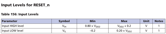
    We are concerned a possibility of violation to 7.1.2.2(input level) in JEDEC
    in considering the case of SoC PVT variation and resistor variation.

    Please let me know the reason of 2.2kΩ.

    EVM


    measurment result
    2.2K is too strong of a pulldown for this signal.  It needs to be 10K.  Please check the latest updates to the AM62P schematic here:  https://e2e.ti.com/support/processors-group/processors/f/processors-forum/1340906/faq-am62p-am62p-q1---custom-board-hardware-design---design-and-review-notes-for-reuse-of-sk-am62p-lp-schematics

    Pull down resistor tolerance on DDR reset_n signal

    What is the required tolerance for 10kohm resistor when considering PVT?

    We don't spec a tolerance for that resistor.  10K was chosen because the previous resistor on our EVMs was 2.2K which proved to be too strong, and the Vih was sometimes not met for DDR_RESET_N.  

    If the tolerance of 10kohm is +/-10%, is it met for DDR_RESET_N?

    yes +/-10% should be adequate

    Implementation reference for LPDDR4

    Implementation example for DDR4 interface 

    Additional inputs: 

    Please let me know the reason that 10kΩPD is OK in no circumstances(device PVT and variation of PD resistance value).
    We can not know the drive strength of this I/O because there is no spec in datasheet.

    This value has been shown in our characterization across PVT to provide a higher voltage level (vs using a 2.2Kohm resistor) when DDR_RESETn is deasserted during initialization. This provides better margin above Vih for that signal.

    We would like the evidence that there is no VIH violation in no circumstances. Please let me know the minimum voltage level in worst condition with PD10KΩ. Or, please let me know the minimum drive level as VOH and IOH.

    We don't specifically test this voltage level across PVT. The IO driver in this mode should be able to achieve VOH=>0.85*VDDQ and VOL=<0.15*VDDQ according to the IP vendor. They have checked this over PVT in simulation.

    AM62P-Q1: Electrical Characteristics Inquiry: VOH/VOL for AM62P LPDDR4 CKE and RESET Pins

    We are currently using LPDDR4 SDRAM in our design with the AM62P device.
    We understand that the DDRSS interface is JEDEC‑compliant for LPDDR4; however, we would like to clarify the electrical characteristics of several specific signals.

    In particular, we would like to know the VOH and VOL levels for the following LPDDR4‑related pins:

    • DDR0_CKE0
    • DDR0_CKE1
    • DDR0_RESET0_n

    These pins are defined within the LPDDR4 interface, but the datasheet does not appear to provide explicit VOH/VOL specifications for each of them.
    Could you please advise where these values are documented, or provide the correct VOH/VOL levels for these pins when operating in LPDDR4 mode?

    We would appreciate your guidance to ensure proper signal‑level verification in our design.

    We don't specify Voh/Vol levels, but we do support JEDEC compatibility, so those output would comply with the Vih/Vih levels required by the memory.  Here is an example from the Micron datasheet, which matches the JEDEC spec:

    We would like to confirm whether the 10 kΩ pull-down resistor on the DRAM RESET pin (P6), as described in the TI guideline, is mandatory, or if other values (e.g., 4.7 kΩ ) can be used.

    In the “LPDDR4 Board Design and Layout Guidelines” for AM62Ax / AM62Px / AM62Dx,Section 2.3 (LPDDR4 Interface Schematics) shows a 10 kΩ pull-down resistor connected to the RESET pin.
    However, the memory vendor’s guideline specifies a 4.7 kΩ pull-down resistor,and we are unsure which value should take precedence in our design.
    Based on the current specifications in the datasheet, we believe that a smaller resistance value than 10 kΩ may also be acceptable in terms of the SoC’s drive capability.

    [Questions]
    I would like to ask about the pull-down resistor value for the DRAM RESET pin.
    Is the 10 kΩ value specified in the guideline mandatory?
    Or would it be acceptable to use a smaller resistor value (e.g., 4.7 kΩ) as long as it functions as a pull-down?If 10 kΩ is recommended or required, could you please explain the reason, including any electrical concerns when using a smaller resistor value?

    Nothing less than 10K is recommended.  A lower value creates a stronger pull down, and the RESET pin driver is not strong enough to overcome this.  We were seeing voltage droops on some boards near the Vih threshold.

    We do not have IO specs for the DDR IOs.  They won't be similar to the other IOs on the device since the DDR interfaces to the DDR PHY with special LVSTL IOs for LPDDR4. When we were debugging the voltage droop issue with DDR RESET, we found that IOHmax@VOH = 1.1mA for the DDR RESET IO.  So we had to increase the pull down to ensure the signal stays high enough away from the threshold.   I don't believe the RESET IO has a dedicated drive strength requirement in JEDEC spec

    Regards,

    Sreenivasa

  • Hi Board designers,

    Inputs related to DDR design guidelines.

    After reading this version of the DDR design guide www.ti.com/.../sprad66b.pdf, I have several confusions.

    1. According to LP4_DRS6 in Table 2-7, the propagation delay of DQSx can be greater than DQ/DM.

    However, in 3.5.3.2, 'DQSx delays must be less than the DQ and DM delays in the respective BYTEx' is mentioned. Which design rules should be followed?

    2. Besides, is LP4_ACRS3 in Table 2-6 too strict compared to LP4_DRS4 in Table 2-7?

    The package delay between DDR0_CK0 and DDR0_CK0_N has exceeded the value LP4_ACRS3. So I want to double confirm.

    3. According to LP4_DRS3 in Table 2-7, does CK delay must be greater than DQS? Is 3*tck too loose?

    1. Yes, the recommendation is that the DQS pair within a byte should have the shortest delay. As mentioned, the design allows for the DQ/DM to be shorter. We are adjusting the wording of the statement in 3.5.3.2 to align with the table

    2. The skew on DQS and CK should be tightly matched as specified in the app note. I confirmed these differential pairs do have different skew requirements as noted in the app note (this was specified by the IP vendor). When performing skew matching, package delays should be accounted for. It is true that the package delay between CK0 and CK0_n is large, but it was recommended by the IP vendor to keep the mismatch in the package, and perform the length matching on the PCB.
    3. Yes, CK delay should be greater than DQS to facilitate write leveling algorithm.

    Is there is no additional skew requirement between DQs within bytes in table 2-7? We follow the 20ps skew between DQs , including the AM62D package. If there is no strict requirement, we can reduce many snake traces.
    LP4_DRS5 in table 2-7 defines a max skew of 150ps. Where are you seeing 20ps?
    20ps is the value we refer to some experience of PCB layout.

    (+) AM62x: SK board DDR_VREFCA circuit - Processors forum - Processors - TI E2E support forums

    On AM62x SK schematic Page 16, what is the purpose of C361 between DDR_VERFCA and VDD_DDR4, is it necessary or helps to stability DDR_VREFCA?

    In app notes: AM64x/AM243x DDR Board Design and Layout Guidelines  page 12, only mentioned to add 0.1uf near to VERFCA pin.

    2.10 VREF Routing JEDEC defines two reference voltages that are used with DDR4 memory interfaces. These are VREFDQ and VREFCA. VREFDQ is the reference voltage used for the data group nets during reads and writes. VREFCA is the reference voltage used for command and address inputs to the SDRAMs. DDR4 SDRAMs generate their own VREFDQ internally. Similarly, the processor's DDR4 PHY generates its own VREFDQ internally. The VREFCA reference voltage must be generated on the board and propagated to all of the SDRAMs. VREFCA is intended to be 50% of the DDR4 power supply voltage and is typically generated with the DDR4 VTT power supply. It should be routed as a nominal 20-mil wide trace with 0.1-μF bypass capacitors near each device connection. Narrowing the VREF trace is allowed to accommodate routing congestion for short lengths near endpoints.

     these caps help filter any noise from the DDR4 supply/ground (C361 and C363).  The additional cap C362 is needed for decoupling near the VREFCA pin of the memory. 

    (+) AM6442: DDR Decoupling Capacitors - Discrepancies between TMDS64EVM Design & TI/Micron Recommendations - Processors forum - Processors - TI E2E support forums

    n reviewing all the documentation from TI & Micron for the DDR4 design, I noticed that the TMDS64EVM Design does not align with the recommendations for almost all the decoupling capacitors for for both the SoC & the DDR device. In particular, I noticed the following:

    1. The EVM does not follow the guidance of TI's "SPRACU1A - AM64x DDR Board Design and Layout Guidelines"
    2. The EVM does not follow the Micron guidelines in "TN-40-40 - DDR4 Point-to-Point Design Guide" which is the Micron equivalent to the above TI document.
    3. The above TI document refers you to the "SPRAC76G - Sitara Processor Power Distribution Networks - Implementation and Analysis" document for the required qty & size of the high speed decoupling caps. The PDN document in turn refers you back to the DDR4 guidelines doc.

    Key points:

    1. Micron recommends 25uF bulk capacitance on VDD(Q) for each DDR device. EVM only has ~22uF.
    2. Micron recommends four smaller bulk caps (to add up to ≥25uF), one in each corner of the device. EVM only has one 22uF in one corner.
    3. Micron recommends 3uF on VPP for each DDR device. EVM only has ~2.4uF.
    4. Micron recommends multiple 1uF capacitors (to add up to ≥3uF), each placed near a VPP pin. EVM only has 2.2uF in one corner
    5. TI recommends a single 22uF bulk capacitance on VDDS_DDR pins. EVM only has ~15uF, made up of 10uF, 4.7uF and 1uF.
    6. Due to the self-referential loop, TI has no explicit requirement or recommendation for the high speed decoupling caps for the SoC.
    7. TI recommends 12 high speed decoupling caps for the DDR device, totalling 850nF (~70nF per cap). The EVM only has 12 x 10nF caps (totalling 120nF).

    I then searched this forum and found 2 posts which have highlighted similar concerns:

    1. AM6442: High-Speed bypass capacitors in the power supply line for DDR
    2. AM6442: bulk capacitors on TMDS64EVM

    In our design, we are hoping to leverage as much of the exact placement and routing of the DDR<->SoC as possible. However, we do not want to compromise the signal integrity, reliability or EMI performance of our product as it is in an application that requires high reliability. As such, we would like to understand the design approach that was taken with the EVM, and the decisions that led to not following the guidelines set out by TI & Micron. It would also be useful to have any test reports/results relating to the DDR & PDN from TI's design verification testing of this EVM, so that these trade-offs can be evaluated.

    Most of the discrepancies you are seeing on the EVM is due to the fact that the EVM was conceived before a lot of the app note was finalized.  We performed full power aware simulations on the EVMs, so even though we technically don't meet the app note requirements, we did pass sims to ensure a robust design.  This is what we would recommend if you are looking for assurances on signal integrity for your application.  I would not rely on strictly various numbers and values of capacitances.

    Do you have the simulations and/or EMC testing results for us to review? In particular, it would be good to see the power consumption figures used for the simulations, so that we can compare against our own design and calculations.

    we are only able to share sim results under NDA. 

    Regards,

    Sreenivasa

  • Hi Board designers,

    Inputs related to DDR size:

    AM623: What is the maximum memory bytes of LPDDR4 that can be used?

    (+) AM623: What is the maximum memory bytes of LPDDR4 that can be used? - Processors forum - Processors - TI E2E support forums

    Regarding the LPDDR4 connection, see
    The [AM62x data sheet] (P1/263) states 4GBytes with LPDDR4, but the [AM62x, AM62Lx DDR Board Design and Layout Guidelines] (P22/44) states Max2GBytes. Which is correct?
    [AM62x, AM62Lx DDR Board Design and Layout Guidelines] (P22/44) states that it is possible to connect the Dual specification with Single.
    In this case, is it necessary to process the pins of the other memory area of LPDDR4?

     it is technically possible to get 4GB of LPDDR4 with AM62x, however, as noted in the Layout guidelines, you would have to use a dual rank, dual channel LPDDR4 and only connect 1 rank to avoid splitting the data bus on the board. Thus, you would not be able to access half of the memory.

    So the layout guidelines suggests that if you are needing more than 2GB of memory, you should use DDR4.

    When using 4GB(Dual) of LPDDR4, do I need to process unused pins?

     you can leave most of the unused pins unconnected. The unused DQS signals on the memory should be pulled to opposite polarity (ie, DQS_t pulled low, DQS_c pulled high) with a 1K resistor

    (+) AM6442: AM6442 support for 12Gb LPDDR4 - Arm-based microcontrollers forum - Arm-based microcontrollers - TI E2E support forums

    Does AM6442 support Micron 12Gb 16bit-bus LPDDR4?

    No, only memories with power-of-2 capacity are supported.

    Regards,

    Sreenivasa

  • Hi Board designers, 

    FYI on connecting DDSS unused pins 

    AM62P: How to handle DDR pins required by only DDR4 when LPDDR4 is used?

    My customer is drawing the schematic of AM62P.

    They have question for DDR pins.

    When using LPDDR4, how should they handle pins that are only used for DDR4? They checked the document "AM62Ax, AM62Px, AM62Dx LPDDR4 Board Design and Layout Guidelines" (SPRAD66B), but could not find the information.

    Their understanding of unused pins when using LPDDR4

    DDR0_a[13:6]

    DDR0_ACT_N

    DDR0_ALERT_N

    DDR0_BA0/1

    DDR0_BG0/1

    DDR0_ODT0/1

    DDR0_PAR

    DDR0_WE_N

    These signals can be left unconnected.  Please refer the SK schematics implementation and follow the same.

    Regards,

    Sreenivasa

  • Hi Board designers, 

    FYI on simulations:

    Could you please answer following questions?

    Our customer is going to run SI simulation on SoC-DDR.

    Could you tell us about the probe point when we simulate with IBIS model?
    Which edge should customer use Die or Pad when at SoC side/Reads?

    DDR4/LPDDR4 read simulations must show margin against the provided eye mask at the SoC DiePad. All other measurements are at the DRAM package pin as defined by the JEDEC spec.

    DDR4/LPDDR4 uses both rising and falling edges of the DQS strobe during reads.

    Refer to AM62x, AM62Lx DDR Board Design and Layout Guidelines https://www.ti.com/lit/an/sprad06c/sprad06c.pdf

    4.5.3.3 Mask Report

    The minimum jitter and noise margins are to be captured with respect to the eye masks. This masks are data
    rate dependent, and includes:
    • Data read eye mask at the SOC die pad for functionality testing.
    • Data write eye mask (JEDEC spec) at the DRAM pin/BGA for compliance testing.
    • CA bus eye mask (JEDEC spec) at the DRAM pin/BGA for compliance testing.

    Table 4-3. LPDDR4 Eye Mask Definitions/Requirements

    Read eye masks are defined here.

    I added additional inputs from the simulation expert:

    There is no concept of “probe point” while creating the IBIS model. It includes the package parasitics along with IO buffer details.

     As regards their question about probe points for simulation, the customer should probe at the SoC die for DDR read simulations and Memory BGA (align with JEDEC) for DDR write simulations.

    Regards,

    Sreenivasa

  • Hi Board designers, 

    FYI on ODT configuration connection

    (+) TDA4VE-Q1: LPDDR4 design guide what the exact value for the pull up res of ODT? - Processors forum - Processors - TI E2E support forums

    TDA4VE-Q1: LPDDR4 design guide what the exact value for the pull up res of ODT?

    From below guide, I can see the resistor value for others, but there is missing the value of ODT_CA_A/B, do we have any recommend value? In EVM, we are using 10K, but I want to double check about this, is it the best value? because from the Sitara AM62P board, we use 2.2K, and some customer is using 1K, so I want to figure it out, what is the best value? can you share some standard (Memory datasheet or JEDC?) customer need to follow, or any pull up resistor value can be accepted?

    Jacinto 7 LPDDR4 Board Design and Layout Guidelines (Rev. F)

    The specific resistor value is not critical - as its not a calibration or termination resistor value.  It is a logic input - so any resistor value can be used as long as it sets the correct logic value. All the resistor values you mentioned (10K, 2.2K, 1K) should all be fine.

    So if this signal is connected to 1.1v, the pull up resistor value is not matter, right? but previously in TDA4VEN EVM, customer connect to 0.55v(pull up to 1.1v with 10K and pull down with 10K), the DDR will have some stability issue (can work in low frequency, but failed in high frequency), and Micron lpddr4 can work in all frequecy, but Samsung and other ddr vendor can't work. this is interesting result if this is just logic input. capture from the micron ddr datasheet, can it be applied to all DDR vendor?


    The signal is an input and the responsibility of the board design is to provide the proper logic high or logic low value.  The mentioned 0.55V was an error because that is an invalid logic level.  That voltage resulted from an on-board pull-up and on-board pull-down....which is a manufacturing mistake and not a valid implementation.  There should be no pull-down resistor on board. 

    The 'weak' internal pull-down resistor and/or leakage current into the input pin may vary across memory manufacturers - so I recommended customer references those datasheets.  (For example - in datasheet I am reviewing, I see no definition of weak internal pull-down, but I do see max input leakage of 4uA).  In general - resistors in range of 1K to 10K should have no issue setting proper logic level for this pin. 

    (+) AM6442: How to use the DDR Subsystem Register Configuration in SysConfig Tool - Processors forum - Processors - TI E2E support forums

    The VREF setting is just the initial setting that the training algorithm starts with.  It should be determined based on the drive strength and termination set.  As an example, for writes, if the default output driver impedance is set to 40ohm, and the termination in the memory is set to 40ohm, the ideal VREF is:

    (VOH - VOL)/2+VOL = (1.2-0.6)/2+0.6=0.9V which is 75% of VOH.  

    The values for various drive strength and termination settings can also be obtained from the DDR datasheet.


    The default values in the tool don't line up exactly to this.  I will make that adjustment in the next revision.  In actuality, any setting around 75% should be fine as this value gets trained to an optimal reference voltage.

    (+) AM6442: How to use the DDR Subsystem Register Configuration in SysConfig Tool - Processors forum - Processors - TI E2E support forums

    By the way, more information can be found for J7. The information for various settings in the DDRSS Register Configuration Tool (Spreadsheet) can be found in the documentation (SPRACU8).

    www.ti.com/.../spracu8a.pdf

    the configuration file you sent is set for a PLL frequency of 200MHz, which translates to a memory clock frequency of 400MHz (or 800MTs).  This is too slow for DDR4 with the DLL enabled

    Please try the attached file, which sets the memory clock frequency for 800MHz (1600MTs)

    /cfs-file/__key/communityserver-discussions-components-files/791/3617.k3_2D00_am64_2D00_ddr_2D00_config_5F00_800MHz.dtsi

    Regards,

    Sreenivasa

  • Hi Board designers, 

    FYI on terminations

    (+) AM67A: How user can set Drive strength/Termination for DDR_CK - Processors forum - Processors - TI E2E support forums

    Termination

    The DDR clock is terminated by the LPDDR4 memory.
    LPDDR4 memory does not have a dedicated ODT configuration for DDR clock. Rather, the CK ODT configuration is shared with the CA and CS signals, and defined by MR11[6:4]. 
    MR11[6:4] is configured by the input "Termination: CA ODT" under the "IO Control B) DRAM IO Configuration" setting. 

    Drive Impedance

    The AM67 DDR register configuration tool does not have a unique DDR clock drive impedance configuration input.
    The DDR clock drive impedance configuration will be set based on the CA drive impedance configuration (parameter "Drive Strength: CA[5:0]" under section "IO Control A) Processor / DDR Controller IO Configuration").

    The reason we use 33-ohm SE/66-ohm DIFF in pace of 40-ohm SE/80-ohm DIFF is because of the T-branch segments on the PCB.  When the trace splits into two segments, to maintain the same impedance seen by the source, the impedance should double.  So a 40-ohm SE trace would become two 80-ohm SE traces.  80-ohms SE trace are typically not achievable on a PCB.  66-ohms SE may not be achievable either but is much closer than 800hms SE.  So the 33-ohm SE/66-ohm DIF might give you better signal integrity.  Each PCB design is different and is up to each customer to simulation and determine best implementation for their design.

    (+) AM2434: Recommended Typ PCB single-ended impedance and differential impedance for DDR and PCIE - Arm-based microcontrollers forum - Arm-based microcontrollers - TI E2E support forums

    1.DDR4 trace impedances

    • Let me ask some other team members about this. My immediate suggestion would be to follow the recommendations in the layout guidelines application note since these are generated based on the results of our DDR controller characterization. 

    Our DDR4 controller and DDR3 memories support a wide range of driver/termination values: 34,40,48,60,80,120,240-ohm. 

    The table PS9 and PS10 are one supported example at the 40-ohm single-ended setting. If the routing is done well, there should be no issue with supporting 50-ohm lines. Most PCB fab will be +/-5% or +/-10% tolerance anyway. The 48-ohm setting would probably be best to start with. 

    2.The PCIe standard dictates the interoperability of root and end-point devices, including the driver/receiver impedance match. 50-ohm single-ended / 100-ohm differential pairs are the standard and should be followed in all designs including the AM243x PCIe. 

    3. The PCIe standard dictates the AC-coupling / DC-blocking nominal capacitance of 100nF. In terms of materials, our characterization systems typically use X7R or better capacitors for these designs so that the differences between capacitors, and over temperature/time does not significantly impact performance. From From a PCB design perspective, the goal is to minimize the impedance discontinuity that the capacitors pads add to the transmission-lines. Using smaller 0201 capacitors can help with this. Also leaving return path voids underneath the capacitors. But you would need to make these PCB design decisions based on a 3D EM field solver or PCB measurements. 

    (+) AM6442: DDR4 Calibration Values - Processors forum - Processors - TI E2E support forums

    IO calibration results are in PHY_1322 to PHY_1331.  Note that these will continually change since periodic IO calibration must enabled in all configurations for normal operation.

    Regards,

    Sreenivasa

  • Hi Board Designers,

    Inputs related to IBIS model probe point:

    Could you tell us about the probe point when we simulate with IBIS model?
    Which edge should customer use Die or Pad when at SoC side/Reads?
    (We wonder the the probe point which defined of spec of Reads.)
    DDR4/LPDDR4 read simulations must show margin against the provided eye mask at the SoC DiePad. All other measurements are at the DRAM package pin as defined by the JEDEC spec.
    DDR4/LPDDR4 uses both rising and falling edges of the DQS strobe during reads.
    Refe to AM62x, AM62Lx DDR Board Design and Layout Guidelines www.ti.com/.../sprad06c.pdf
    4.5.3.3 Mask Report
    The minimum jitter and noise margins are to be captured with respect to the eye masks. This masks are data
    rate dependent, and includes:
    • Data read eye mask at the SOC die pad for functionality testing.
    • Data write eye mask (JEDEC spec) at the DRAM pin/BGA for compliance testing.
    • CA bus eye mask (JEDEC spec) at the DRAM pin/BGA for compliance testing.
    Table 4-3. LPDDR4 Eye Mask Definitions/Requirements
    Read eye masks are defined here.

    I was getting eye diagrams that look like the image pasted below. I have since found that it is a lot cleaner when using the die-side probing option in my simulation software. Models from the last interface I simulated did not have a built in package model, so I wasn't aware you could do that.


    It makes sense that die side probing would be what we'd ultimately care about. Let me know if that is not how it is intended to be used though.

    There is no generic guideline that can be given. Different simulations require different points at which the signal needs to be probed and also with different specifications.

    For e.g. the DDR JEDEC specifications for Write transactions require waveforms to be measured at the DRAM BGA, whereas the Read transactions require waveforms to be measured at the SoC Die.

    (+) [FAQ] AM620-Q1: Inputs required for DDR4 Signal Integrity Simulation - Processors forum - Processors - TI E2E support forums

    CA(Command/Address) Mask - DDR4 @ DRAM Die Pad 1600MT/s
    Shape    Trapezoid
    Height     Vrefca+/-100mV(setup),Vrefca+/-75mV(hold)
    Width     366ps + SR Derating (0.29280 tCK for 0 derating)

    Write Mask - DDR4 @ DRAM Die Pad 1600MT/s
    Shape    Rectangle
    Height     136mV
    Width    180.2ps (0.28832 UI)


    Read Mask - DDR4 @ SOC Die Pad 1600MT/s
    Shape    Hexagonal
    Height    VdIVW 136mV
    Width    
            TdIVW1 323.6ps (0.51776UI)
            TdIVW2 187.6ps (0.30016UI)

    (+) AM625: DDR4 Address and Clock routing (matching) - Processors forum - Processors - TI E2E support forums

     The app note is intentionally strict in its requirements, and skew between addr/ctrl and clock for DDR4 needs to be tightly controlled.  In practice, since the max freq for the interface is 800MHz (much lower than JEDEC maximum), you can relax these requirements (as the EVM shows), but it is advised that you perform board simulations to ensure proper signal integrity.  If you are not doing any simulations, it is best to maintain the requirements that are in the app note.

    (+) AM623: Conception clarification for (LP)DDR4 training Algorithm - Processors forum - Processors - TI E2E support forums

    1) Yes, both DDR4 and LPDDR4 require training at the highest supported frequencies.  This helps optimize signal timing and VREFs for greatest margin

    2) Yes, training is performed by the DDR IP

    3) Yes, currently shmoo tool only supports LPDDR4.  Support for DDR4 is in development

    4) It just means that certain training step are only applicable for DDR4 or LPDDR4.

    5) This just means after initialization has been completed, when read/writes or typical activity like refreshes are being performed with memory.  Periodic training is intended to be performed during normal operation of the DDR so that things like calibration, training updates, etc. can be completed as background tasks.

    (+) AM623: Boot log for memory bring up on a AM6234ATGGHAALW - Processors forum - Processors - TI E2E support forums

    he following training step are performed during initialization:

    • Enables the following training algorithms during DRAM initialization:
      • IO calibration of the controller/PHY
      • Command Bus Training (CBT), including reference voltage programmed in MR12 of DRAM
      • CA/CS leveling
      • Write leveling
      • Read Gate Training
      • Read Leveling (Read Data Eye Training)
      • VREF Training
      • Write DQ Leveling (Write Data Eye Training)

    We don't specifically document the training results, as much of the information is encoded and not very useful to the end customer.  Ti can support decode  training results if that will help you.  Otherwise, the Eye Tool will provide the best view overall of the training results and margin.  I would also recommend performing memory stress tests across your expected temp range to give more confidence on your board design.

    The default DDR configuration is setup to support WDQS Control Mode 1 - Read-based control.  The training is performed at every boot cycle when the initial bootloader executes.  

    Is your customer trying to debug an issue?  If so, have them send the DDR part number and DDR configuration (.dtsi and .syscfg from the DDR Register Configuration Tool) and i can help check to see if their configuration is correct.

    Also, they can add the patch descirbed in Section 2 here:  [FAQ] Board bring up tips for Sitara devices (AM64x, AM243x, AM62x, AM62L, AM62Ax, AM62D-Q1, AM62Px) 

    which will help output the DDR registers after training, and post here.

    (+) AM6442: DDR Qualification DDR4 - Processors forum - Processors - TI E2E support forums

    (+) AM625: DDR4 Trace Impedance and Drive Strength - Processors forum - Processors - TI E2E support forums

    for lightly loaded signals (ie, point to point), 50ohm single ended (100ohm differential) trace impedance is acceptable, controller does support 48ohm drive strength setting.  Just watch out for manufacturer tolerances which can be as much as +/- 10%, and some manufactures have difficulty with the thinner traces.

    (+) AM625: How to configure DDR4 with 2 DDR4 chip of 4GB - Processors forum - Processors - TI E2E support forums

    the MT40A4G8NEA-062E:F device that you are using is a dual rank device.  Each package is 8-bit wide.  Thus the sysconfig tool should be configured as such:

    Data Bus Width (per device) 8
    Density (per device) (Gb) 32

    Chip Selects / Ranks 2

    (+) AM625: Can AM62x support 8GB DDR4 physically? - Processors forum - Processors - TI E2E support forums

    (+) AM6252: DDR4 and NAND Flash performance testing - Processors - INTERNAL forum - Processors - INTERNAL - TI E2E support forums

    For DDR4, it is a good idea to run board level tests with memtester overnight and sweep operating temperature between min/max (or even -5% below min and +5% above max).  Another good test is to boot at lowest temp and ramp to highest temp (and vice versa) while running memtester.  This gives a good stress over the operating temp of the application.

    We don't have anything specific for NAND, other than setting up your own test.  If you are booting from NAND, you may want to setup a multiple boot test across temperature to ensure robustness

    The margin tool alone is usually not the definitive answer to validation for most customers, even for LPDDR4. Typically DDR validation starts with board level simulation using the IBIS models of the processor + DRAM and board extraction parameters from the customer's board. Once actual boards are available some do physical eye diagram measurements and the majority of them often run memtester through their own defined validation flow. This can be with several boards overnight or even several boards through temperature chambers cycling; customers usually already have multiple checkpoints when it comes to DDR validation.

    (+) AM62L: AM62L Custom Board (DDR4 @800MHz): kernel crashes when executing tar or similar extraction commands - Processors forum - Processors - TI E2E support forums

    (+) AM6412: DDR4 unused pins - Processors forum - Processors - TI E2E support forums

    (+) AM623: Layout differences between LPDDR4/DDR4 RE: CRC - Processors forum - Processors - TI E2E support forums

    CRC is not apart of the JEDEC LPDDR4 specification, so there's no standard hardware support for it in LPDDR4 or the controller. If you want to do CRC checking on the data stored in DRAM, it'd be in an higher level software abstraction layer. From the perspective of an ARM core, bit swizzling/byte swapping is invisible (it's all handled in the DDR IP itself).

    You are correct about in-line ECC being present, this is hardware managed ECC that basically stores the ECC codes inside the DRAM (so living side by side with data) and it uses these codes for single error correction+ double error detection (SECDED). This reduces the amount of DRAM available but allows for error checking to be done by hardware.

    e2e.ti.com/.../5093776

    e2e.ti.com/.../processor-sdk-am64x-ddr-ecc-overhead
    Yes, the answer will depend on cache hit/miss. Minimum throughput impact is 12.5% (with cache hit). With cache misses, impact may be up to 100% depending on the alignment of the transfer.
    e2e.ti.com/.../5037599
    e2e.ti.com/.../am6442-dose-am64x-ddr-subsystem-allowed-32-bit-lpddr4
    Yes, this is allowed. You can use a 32-bit memory and not connect the upper 16bits. Just note that you would not be able to access half of the memory.
    e2e.ti.com/.../4995731
    Your 1GB and 2GB definitions are correct, but the 4GB and 8GB variants are wrong. For scenarios less/equal to 2GB you typically only have 1 entry for 'reg'. For scenarios with more memory, you typically have two. One memory region that starts at 0x8000_0000, and another one (the larger one) starting at 0x8_8000_0000.

    Here's an example for 4GB:
    git.ti.com/.../k3-am62a7-r5-sk.dts
    And here's an example for 8GB:
    git.ti.com/.../k3-am62p5-sk.dts

    e2e.ti.com/.../am6422-am64-support-2-2gb-ddr4-total-4gb
    e2e.ti.com/.../processor-sdk-am64x-ddr-clocks-and-resets
    e2e.ti.com/.../processor-sdk-am64x-no-pbist-for-ddr
    e2e.ti.com/.../5139266
    e2e.ti.com/.../am6424-max-lpddr4-memory-restricted-to-2gb
    AM64x is limited to 2GB by design. Addressing beyond 2GB requires extended addressing (ie, more than 32bits), which is only available in AM62x.

    Regards,

    Sreenivasa

  • Hi Board Designers,

    Inputs related to DDR4 termination

     https://e2e.ti.com/support/power-management-group/power-management/f/power-management-forum/1077042/faq-tps51200-supported-applications 

    The number of DIMMs that a single device can support depends on the current requirements of each DIMM. This information should be provided on the datasheet for the individual DIMMs. For more information on determining termination current, see this source: https://www.ti.com/lit/an/slua886a/slua886a.pdf?

    The TPS51200 family of devices are ideal for VTT applications in DDR-DDR4 systems. However, they can be used for any other application where a 2A-3A LDO is necessary. The added bonus of using these devices is that they are capable of both sinking and sourcing current, making them perfect for DDR VTT applications.

    Regards,

    Sreenivasa 

  • Hi Board Designers,

    Inputs related to DDR4 size 

     https://e2e.ti.com/support/processors-group/processors/f/processors-forum/1336276/am623-differences-ddr4-lpddr4-ddrss-am64x-vs-am6232/5093776 

    AM62:

    Table 5-1:

    AM64:

    Table 5-1

    e2e.ti.com/.../processor-sdk-am64x-ddr-ecc-overhead
    Yes, the answer will depend on cache hit/miss. Minimum throughput impact is 12.5% (with cache hit). With cache misses, impact may be up to 100% depending on the alignment of the transfer.
    e2e.ti.com/.../5037599
    e2e.ti.com/.../am6442-dose-am64x-ddr-subsystem-allowed-32-bit-lpddr4
    Yes, this is allowed. You can use a 32-bit memory and not connect the upper 16bits. Just note that you would not be able to access half of the memory.
    e2e.ti.com/.../4995731
    Your 1GB and 2GB definitions are correct, but the 4GB and 8GB variants are wrong. For scenarios less/equal to 2GB you typically only have 1 entry for 'reg'. For scenarios with more memory, you typically have two. One memory region that starts at 0x8000_0000, and another one (the larger one) starting at 0x8_8000_0000.

    Here's an example for 4GB:
    git.ti.com/.../k3-am62a7-r5-sk.dts
    And here's an example for 8GB:
    git.ti.com/.../k3-am62p5-sk.dts

     https://e2e.ti.com/support/processors-group/processors/f/processors-forum/1597066/am6422-am64-support-2-2gb-ddr4-total-4gb
    e2e.ti.com/.../processor-sdk-am64x-ddr-clocks-and-resets
    e2e.ti.com/.../processor-sdk-am64x-no-pbist-for-ddr
    e2e.ti.com/.../5139266

    Can you confirm, that AM62x (acc. to DS) can address 4GB LPDDR4 but AM64x only 2 GB LPDDR4  (acc. to DS) ? What is root cause for this ?

    AM64x is limited to 2GB by design.  Addressing beyond 2GB requires extended addressing (ie, more than 32bits), which is only available in AM62x.

    Regards,

    Sreenivasa

  • Hi Board Designers, 

    Inputs related to the System Configuration (AM62P-Q1) setting value of DDR configuration

    I checked the latest DDR Configuration and found the following three new settings:
    - Enable DRAM Temperature Polling
    - System Temperature Gradient Maximum (C/s)
    - System Response Delay (ms)

    image.png

    I have a question about the newly added settings:
    1. How did you set these settings in previous versions?
        Please let me know the values ​​for each.
    2. Is it recommended to enable or disable DRAM Temperature Polling?
    3. If enabling DRAM Temperature Polling is recommended, have you tested its operation?

    this feature is available in SDK11.02, which is available now on ti.com for AM62P.  

    We performed temperature testing on our EVM to ensure the dynamic refresh rate change occurred correctly across 25C to 125C.  It is encouraged that the customer perform their own testing to ensure proper response time based on their use case.  

    I understand, thank you for your reply.
    If DRAM Temperature Polling is disabled, what are the settings for the following two items?

    - System Temperature Gradient Maximum (C/s)
    - System Response Delay (ms)

    I would also appreciate it if you could explain the relationship between the DRAM Temperature Polling settings and the above items.

    If DRAM Temperature Polling is disabled, what are the settings for the following two items?

    - System Temperature Gradient Maximum (C/s)
    - System Response Delay (ms)

    if temp polling is disabled, the values for those parameters are irrelevant and can be set to any value

    System Temperature Gradient Maximum:  this is the maximum rate of temperature change your application is expected to experience.  For example, the default value of 3C/s means that you don't expect the temperature to change more than 3C per second.  This will help determine how often the system needs to check the DDR temp sensor

    System Response Delay:  this is how fast your application can respond to the DDR interrupt that is associated with the read of MR4 temp sensor.  An interrupt will be generated when the DDR requests a refresh rate change due to temperature.  The response time to this request will also help determine how often the system needs to check the DDR temp sensor.

    Both values help calculate the hardware timer with determines how often the DDR controllers check the MR4 register.

    I understand that if temperature polling is disabled, the two items are ignored.

    Regards,

    Sreenivasa

  • Hi Board Designers, 

    Inputs related to custom board debug related to DDRSS.

    (+) AM625: Custom design - Troubleshooting a no boot issue - Processors forum - Processors - TI E2E support forums

    Please follow the below FAQ as i review the schematics

    (8) [FAQ] Board bring up tips for Sitara devices (AM64x, AM243x, AM62x, AM62L, AM62Ax, AM62D-Q1, AM62Px) - Processors forum - Processors - TI E2E support forums

    I have checked all the PMIC output and all the voltage levels are correct.  I cannot change the bootmode resistors, unfortunately, but they are working correctly..   I do see the initial boot messages from SD Card. 
     
    I looked at your FAQ and this appears to be part of Section 2.  I am going to review this section in greater detail and see if I can resolve it.

    You cannot see the pullups for the SD card on the schematic because they are inside the ESD device. 
    EMIF06-MSD02N16. www.st.com/.../cd00217829.pdf

    "The EMIF06-mSD02N16 is a dedicated interface device for micro SD card/T-Flash card. The device provides:
    • ESD protection
    • EMI filterering
    • Pull-up resistors
    • Card detection circuit"

    Based on this FAQ you sent me:

     [FAQ] Board bring up tips for Sitara devices (AM64x, AM243x, AM62x, AM62L, AM62Ax, AM62D-Q1, AM62Px) 

    I have looked at section 2.  I have implemented the DDR register Dump, and the memory test.  I am definitely seeing some issues with the DDR4 memory.
    memtest_reg.txt

    Would you take a look and advise?

    I have solved the issue!  The voltage divider for VREFCA had a floating ground, making it have full (1.2V). I attached a ground and my memory boot issues are cleared.

    https://e2e.ti.com/support/processors-group/processors/f/processors-forum/1662521/am62l-linux-sdk-ddr-margin-firmware/6427036

    I wanted to share a significant update from our DDR investigation.

    Based on our earlier discussions, we began looking more closely at the DDR electrical configuration rather than the timing parameters. One observation that stood out was that our PCB routing is substantially shorter than the TI SK-AM62 reference design. That led us to investigate whether the default SysConfig drive strength and termination settings might be better suited to the reference board than to our custom layout.

    As an experiment, we modified the DDR electrical settings in SysConfig, rebuilt the R5 bootloader, and programmed the new tiboot3.bin onto one of our worst-case boards (E0018). The changes included increasing the processor DQ/DQS/DM and address/control/clock drive strength to 60 Ω, setting the processor ODT to 80 Ω, configuring the DRAM output driver to RZQ/5 (48 Ω), setting RttNOM to RZQ/6 (40 Ω), and disabling dynamic ODT.

    The results have been very encouraging. E0018, which had consistently failed memtester and our Linux tar extraction/checksum stress test, now successfully trains, boots Linux, completed its first-ever full memtester pass, and has also passed multiple iterations of the tar extraction/checksum test without errors. While we still need to validate this over temperature and across additional boards, this is the first configuration change that has produced a measurable improvement in memory stability.

    At this point, we're planning to characterize this configuration over temperature and repeat the testing on additional boards to determine whether the improvement is consistent across the population.

    From your experience with the AM62x DDR PHY, are there other electrical parameters you would recommend evaluating in addition to the drive strength and ODT settings? For example, are there other impedance, slew rate, VREF, or PHY configuration parameters that you have found to be particularly important when moving from the TI reference layout to a significantly different PCB topology? We'd appreciate any guidance on which settings are most likely to further improve margin.

    Regards,

    Sreenivasa

  • Hi Board Designers, 

    Inputs related to bit swapping

    e2e.ti.com/.../am625-ddr4-bit-swapping-validation
    originally, the tool did not have the capability to define the pin swapping. For normal DDR4 operation, this is ok, since the training is performed over the address signals, and swapping DQ bits within a byte for normal data transactions would not be an issue (writing swizzled data would just read back with the same swizzle)

    But if you wanted to try to read MR registers or other functions which require understanding of data bit swapping, then you would need to define the bits, so this capability was added.

    So depending on your needs, you can choose to ignore the swizzle definition.

    e2e.ti.com/.../am623-please-help-confirm-whether-ddr-meets-the-requirements
    Fly-by
    www.ti.com/.../sprabi1d.pdf
    Again, an important point is that the parallel termination should be placed at the last SDRAM in the fly-by or
    daisy-chained architecture. Each trace to the respective termination should be ≤ within 500 mils and the opposite
    side of the termination resistor should tie directly to the VTT rail.

    e2e.ti.com/.../am67a-importance-of-ddrss-register-configuration-tool-for-bring-up-custom-board
    The difference between the two boards is that they use different DDR memories. How important is it to configure DDR in SysConfig for Linux to bring-up and running?
    It depends on what is different between the memories. If the memories have the same architecture (ranks, channel density, etc.), then it is possible the same configuration may work (though maybe tweaks to IO settings might be required). However, it would be very important if the memories do not have the same architecture.

    Can Linux still boot even if the configuration is wrong?
    If you have a non-working DDR interface or unstable DDR interface, likely Linux (or any other software executing out of DDR) would not boot.


    Due to LPDDR4 data bus wiring, BANK2 and BNAK3 are SWAPPED. Is it necessary to swap BANK0 and BANK1 accordingly?
    Could you teach me an example of connection when swapping only BANK2 and BANK3.
    Be sure to review the DDR layout guidelines app note which has recently been updated: www.ti.com/.../sprad66
    If you are swapping banks, you will need to generate a new configuration using the sysconfig tool. If you swap banks 2/3, you don't necessarily have to swap 0/1. The app note will have the rules on data bit/byte swapping

    LPDDR4
    e2e.ti.com/.../3856783

    I have some questions regarding the LPDDR4 interface:

    1. Data pin swapping: Not only are data lines swapped within a byte, but the DataMask (DM) lines are swapped as well. Is this possible because the assignment per byte (DQ & DM) can be configured individually?
    2. CLK impedance: I also noticed that the CLK signal is routed with an impedance of only differential 66 ohm. What is the reason for this impedance value?


    yes, DQ and DM signals within a byte can be swizzled.  This can be defined in the DDR register configuration tool:

    For the CLK impedance, this is what we specify in the DDR Layout Guidelines: https://www.ti.com/lit/pdf/sprad66

    Also see note 5, which explains that since the CLK and address signals have to be T-branched on board, the impedance should be div-by-2 for the branched portion of the trace.

     https://e2e.ti.com/support/interface-group/interface/f/interface-forum/1627853/am62p-q1-dqs-connection-between-am62p-and-lpddr4 

    Regards,

    Sreenivasa

  • Hi Board Designers, 

    Inputs related to recent debug

    (+) AM625: Custom design - Troubleshooting a no boot issue - Processors forum - Processors - TI E2E support forums

    The voltage divider for VREFCA had a floating ground, making it have full (1.2V). I attached a ground and my memory boot issues are cleared.

    Regards,

    Sreenivasa

  • Hi Board Designers, 

    Inputs related to Spread Spectrum Support for DDRSS 

    (3) AM62A3: AM62A34ASMSIANFRQ1 DDR4 clk RE issue - Interface forum - Interface - TI E2E support forums

    we are using AM62A34ASMSIANFRQ1 , the DDR4 clk is set as 800MHZ ,and we find that the harmonic frequece 1.6G is above the limit during EMC RE test . 

    we had enable DBI . and we find the PLL support SCG , can we set SCG enable? how to set it ? 

    image.png

    Spread spectrum is not supported for DDR PLL.  You can possibly mitigate the harmonics by slightly changing the DDR frequency to 790MHz for example.

    BTW, speed grade of the AM62A you are using is capable of max DDR frequency of 1600MHz.  So you could run at 1580Mhz for example.  Use the DDR Register Configuration Tool to change the DDR configuration for the new frequency: dev.ti.com/.../

    Refards,

    Sreenivasa